A gallium nitride-based semiconductor light-emitting tube with a p-type active region

A gallium nitride-based, active region technology, applied in the field of gallium nitride-based semiconductor light-emitting tubes, can solve problems such as uneven carrier distribution, low minority carrier injection efficiency, and limited number of quantum wells

Inactive Publication Date: 2011-12-14
XIAMEN UNIV
View PDF5 Cites 14 Cited by
  • Summary
  • Abstract
  • Description
  • Claims
  • Application Information

AI Technical Summary

Problems solved by technology

In intrinsic gallium nitride-based materials or N-type gallium nitride-based materials, holes are used as minority carriers, but the diffusion length of holes as minority carriers in gallium nitride-based materials is much shorter than that of electrons as minority carriers, and the minority carrier diffusion The short length will affect the optoelectronic characteristics of semiconductor devices, such as: the uneven distribution of carriers in the active re

Method used


Image

  • A gallium nitride-based semiconductor light-emitting tube with a p-type active region
  • A gallium nitride-based semiconductor light-emitting tube with a p-type active region
  • A gallium nitride-based semiconductor light-emitting tube with a p-type active region

Examples


Embodiment 1

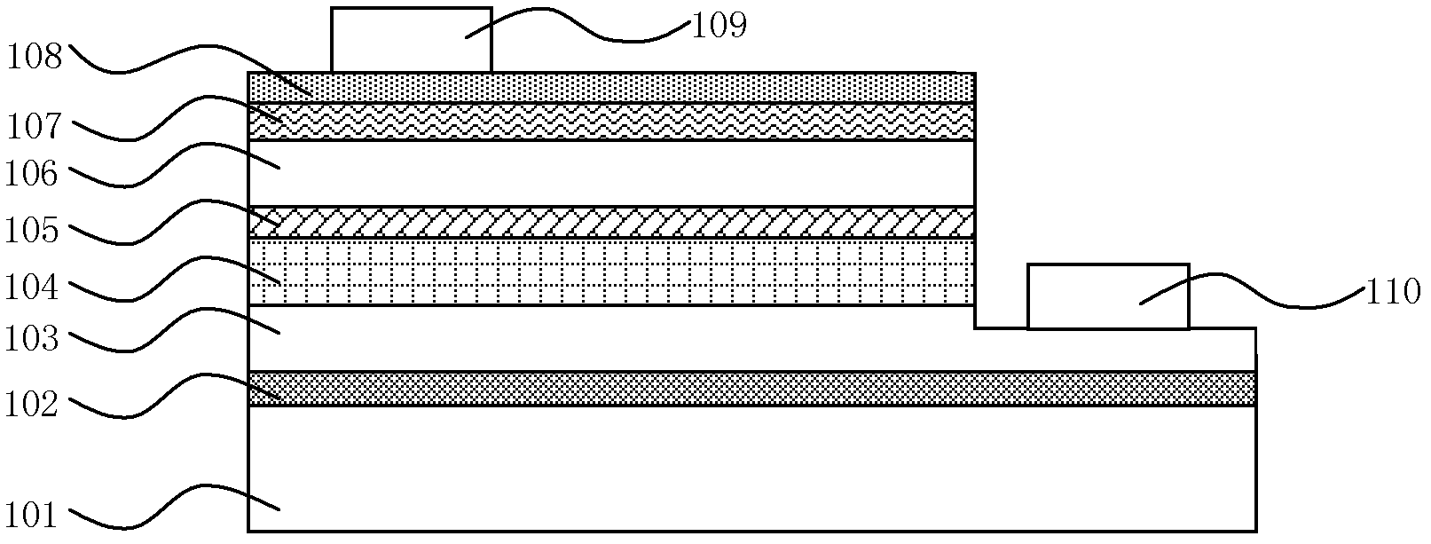
[0027] Place the sapphire substrate (101) in the MOCVD reaction chamber, first raise the temperature of the reaction chamber to 600-1100°C, preferably at 1100°C, and bake the substrate in a hydrogen atmosphere to remove surface impurities. In the range of 600~1100℃, use NH 3 or NH 3 with H 2 The mixed gas is used to treat the substrate surface.

[0028] The temperature of the reaction chamber is lowered to within the range of 550-560° C., preferably 560° C., and the Ga source and the N source are supplied to grow a buffer layer (102) with a thickness of 20-30 nm.

[0029] The temperature of the reaction chamber is raised to 1040-1080°C, and the Ga source and N source are introduced to grow a 2 μm thick non-doped GaN material, and then the reaction chamber is added with a Si source to grow a 2 μm thick N-type doped GaN material ( 103).

[0030] Cool the reaction chamber to 650-900°C, preferably 700-850°C, and grow 4 cycles of In x Ga 1-x N(202, 0x Ga 1-x N as a potential...

Embodiment 2

[0038] The specific implementation method of Embodiment 2, except that the structure of the active region is different from that of Embodiment 1, other parts can use the same process steps, which will not be repeated here. The following only introduces the manufacturing process of its active region structure.

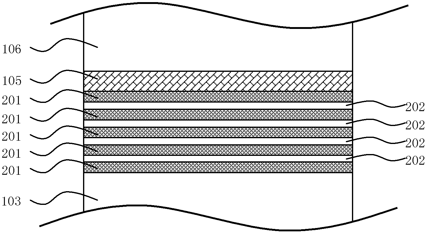
[0039] After the growth of the N-type GaN material (103) is completed, the temperature of the reaction chamber is lowered to within the range of 650-900° C., preferably 700-850° C., and four cycles of In x Ga 1-x N(202) / GaN(201) multiple quantum well structure (104, active region). Specifically, the reaction chamber is fed with Ga source and N source to grow the GaN barrier layer, the thickness of the barrier layer is in the range of 2-50nm, preferably 3-20nm, and the Mg source is used as a P-type dopant during the growth process of the GaN barrier layer. Growth potential well layer In x Ga 1-x Ga source, N source, and In source are connected to the reaction chamber...


PUM

PropertyMeasurementUnit
Single layer thicknessaaaaaaaaaa
Thicknessaaaaaaaaaa

Abstract

The invention relates to a gallium nitride-based semiconductor light-emitting tube with a P-type active region, relating to a semiconductor light-emitting tube. A substrate layer, a buffer layer, an N-type layer, an active region, a P-type layer, a P metal electrode, and an N metal electrode are sequentially provided from bottom to top; the P metal electrode is connected to the P-type layer, and the N metal electrode is connected to the N-type layer. The active region is sandwiched between the P-type layer and the N-type layer, and the active region is formed by alternately stacking barrier layers and potential well layers including at least 2 stacking periods, and each stacking period includes One potential barrier layer and one potential well layer, the potential barrier layer is doped with P-type dopant. By introducing a barrier layer containing P-type dopants, the luminous efficiency of the active region of the device is improved, the photoelectric performance of the device is optimized, and the purpose of improving the luminous efficiency of the GaN-based compound semiconductor light-emitting device is achieved.

Description

technical field [0001] The invention relates to a semiconductor light-emitting tube, in particular to a gallium nitride-based semiconductor light-emitting tube with a P-type active region. Background technique [0002] With the rapid development of new technology, new technology and new materials, the third-generation semiconductor materials represented by gallium nitride (GaN) and its compound semiconductors, SiC and other materials are widely researched and applied, especially gallium nitride The application of semiconductor materials represented by the series compounds in the field of optoelectronics, such as blue-green light and ultraviolet light-emitting diodes, blue-green light and ultraviolet lasers, short-wavelength solar cells, photodetectors, etc., has broad prospects and development potential. Some finished devices have been widely used in high-power lighting, full-color outdoor large display screens, optical communications, storage, etc. ([1] Shuji Nakamura.Recen...

Claims


Application Information

Patent Timeline
IPC IPC(8): H01L33/06H01L33/32
Inventor 刘宝林曾凡明刘威
Owner XIAMEN UNIV
Why Eureka
Try Eureka