Preparation method of nano-imprint template in vector type AFM (atomic force microscopy) nano processing system

A nano-fabrication and nano-imprinting technology is applied in the manufacture of microstructure devices, metal material coating processes, and processes for producing decorative surface effects. It can solve problems such as restricting the development of nano-imprinting technology and achieve good control The effect of stability and stability, high processing accuracy, and loose processing environment

Inactive Publication Date: 2012-01-04
SHANGHAI JIAO TONG UNIV
View PDF3 Cites 9 Cited by
  • Summary
  • Abstract
  • Description
  • Claims
  • Application Information

AI Technical Summary

Problems solved by technology

However, the preparation technology of the template, the soul of the current ...

Method used


Image

  • Preparation method of nano-imprint template in vector type AFM (atomic force microscopy) nano processing system
  • Preparation method of nano-imprint template in vector type AFM (atomic force microscopy) nano processing system
  • Preparation method of nano-imprint template in vector type AFM (atomic force microscopy) nano processing system

Examples


Embodiment 1

[0040] This embodiment mainly includes the following steps:

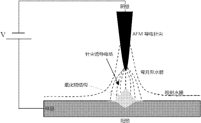
[0041] The first step, sample preparation. The improved RCA cleaning scheme was used to prepare the surface hydrogen-passivated silicon wafer samples to prevent the samples from being easily oxidized when exposed to the atmosphere, and to make the surface roughness of the cleaned samples around 0.1nm;

[0042] The second step is to fix the prepared silicon wafer sample on the object carrier with copper conductive glue or conductive silver paste, put it on the AFM stage, select the appropriate conductive probe according to the conductivity of the sample, and install the probe frame , turn on the switch of the vector AFM nano-processing system, and wait for the temperature and humidity and the AFM circuit processing system to reach a stable state. A digital multimeter for measuring physical quantities such as weak currents, warming up the instrument and waiting for it to stabilize;

[0043] The third step is to carr...

Embodiment 2

[0082] Contact mode processing under the application of a constant electric signal, at this time, the system's own DC signal can also be used for field-induced processing.

[0083] The first step, sample preparation refers to Example 1.

[0084] The second step is to fix the prepared silicon wafer sample on the object carrier with copper conductive glue or conductive silver paste, put it on the AFM stage, select the appropriate conductive probe according to the conductivity of the sample, and install the probe frame , turn on the switch of the vector AFM nano-processing system, and wait for the temperature and humidity and the AFM circuit processing system to reach a stable state. A digital multimeter for measuring physical quantities such as weak currents, warming up the instrument and waiting for it to stabilize;

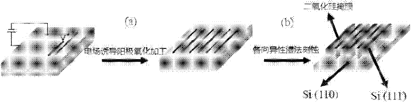
[0085] The third step is to program the required nanostructure, and the program controls the movement of the probe tip.

[0086] According to the geometric shap...

Embodiment 3

[0104] Percussion-mode processing under application of a steady-state electrical signal.

[0105] The first step and the second step of the process are the same as in Example 2, and the third step of the process is the same as in Example 1.

[0106] The fourth step, AFM enters the imaging mode scanning state, set the appropriate scanning range (1 μm ~ 50 μm), scanning rate (0.1 μm / s ~ 1 μm / s), integral gain (for AFM contact mode: ~ 2.00, for knocking mode : ~0.30), proportional gain (for AFM contact mode: ~3.00, for tapping mode: ~0.50) and probe oscillation amplitude and other parameters, and then start scanning the sample surface, so that the stability and repeatability of the scanning image can be achieved. most;

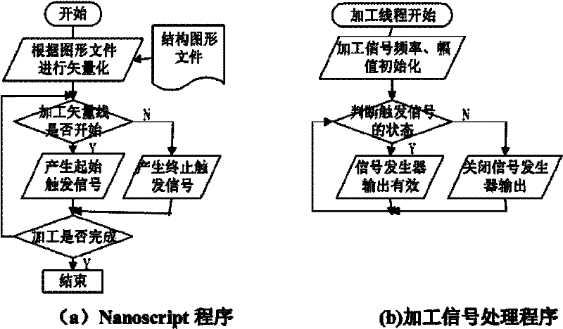
[0107] Step 5. After the scanning process is stable and a stable and repeatable scanning image is obtained, enter the script program mode, call out the Nanoscript interface and then call the previously edited processing macro file to control the waveform and dut...


PUM

PropertyMeasurementUnit
Surface roughnessaaaaaaaaaa
Surface average roughnessaaaaaaaaaa
Roughnessaaaaaaaaaa

Abstract

The invention discloses a preparation method of a nano-imprint template in a vector type AFM (atomic force microscopy) nano processing system, and belongs to the technical field of nano manufacturing. The method comprises the following steps that: the vectorization programming is performed on a required nano structure to obtain a macro document to be processed to control the movement of a pinpoint; the AFM enters an imaging mode scanning state, then begins scanning a sample surface, enters a script program mode after the scanning procedure is stable and a stable scanning image with good repeatability is obtained, invokes and imports the macro document (to be processed) obtained in the third step to a processing system to process; and the AFM enters a real-time imaging mode after the processing is finished, scans again to obtain a surface topography structure image of a processed structure, and finally uses a prepared nano pattern structure as a mask to transfer the nano structure image prepared by the anodic oxidation induced by an AFM electric field by combining with a high-selectivity anisotropism wet etching technology so as to manufacture the nano structure template.

Description

technical field [0001] The present invention relates to a method in the fields of nano-manufacturing and nano-optoelectronic devices, and in particular to a method for preparing a nano-imprint template based on a vector AFM nano-processing system, that is, in a vector AFM (atomic force microscope) nano-processing system Next, the nanoimprint template was prepared by using the electric field-induced anodic oxidation processing method combined with the high-selectivity anisotropic wet etching technology. Background technique [0002] Since the 1980s, Scanning Probe Microscope (SPM) represented by Scanning Tunneling Microscope (STM) has developed rapidly. It is characterized by high resolution and can work in vacuum, atmosphere and liquid environment. has been widely used. Over the past three decades, SPM has developed into a powerful surface analysis tool, greatly expanding the space of surface information research, and playing an important role in promoting the development o...

Claims


Application Information

Patent Timeline
IPC IPC(8): B81C1/00
Inventor 王庆康胡克想王阳培华万霞
Owner SHANGHAI JIAO TONG UNIV
Why Eureka
Try Eureka