GaN-based LED epitaxial wafer and growing method thereof

An LED epitaxial wafer, n-type technology, applied in the direction of gaseous chemical plating, coating, electrical components, etc., can solve the problems affecting crystal quality, reducing luminous efficiency and antistatic ability, etc., to expand current and improve antistatic ability. and leakage, the effect of improving the quality of crystal growth

Inactive Publication Date: 2012-01-25
DALIAN MEIMING EPITAXIAL WAFER TECH
View PDF4 Cites 11 Cited by
  • Summary
  • Abstract
  • Description
  • Claims
  • Application Information

AI Technical Summary

Problems solved by technology

[0005] In the traditional GaN-based LED epitaxial wafer growth method, the InGaN / GaN multi-quantum well layer (Group III Nitride compound semiconductor light-emitting device and method for producing the same. Patent No.: US2010 / 0078660 A1) will be directly grown after the n-type GaN layer ), so that the defects formed by heteroepitaxy or n-type doping will continue to grow in the quantum well, which affects the quality of the crystal itself and reduces the luminous efficiency and antistatic ability of the LED

Method used


Image

  • GaN-based LED epitaxial wafer and growing method thereof
  • GaN-based LED epitaxial wafer and growing method thereof

Examples


Embodiment 1

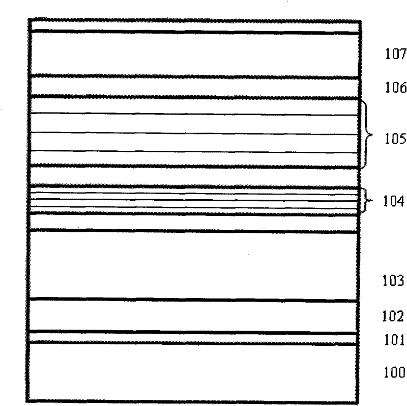
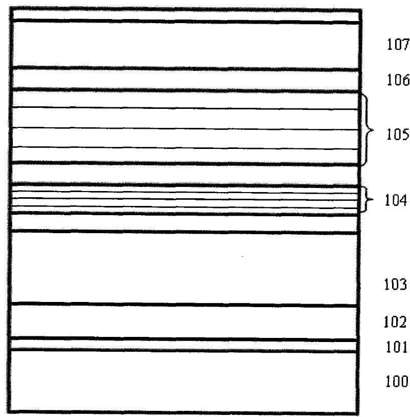
[0040] Embodiment 1 uses the MOCVD method to grow sequentially from bottom to top:

[0041] 1. Put the sapphire substrate with (0001) crystal orientation into the reaction chamber, and then 2 Heating to 900° C. under atmosphere and baking for 20 minutes to purify the substrate at high temperature.

[0042] 2. Lower the temperature to 500°C to grow a low-temperature GaN buffer layer with a thickness of 15nm.

[0043] 3. Grow non-doped GaN with a thickness of 1 μm at 900°C.

[0044] 4. Grow n-type GaN with a thickness of 1 μm at 900°C.

[0045] 5. An n-type GaN defect blocking layer is grown for one cycle at 900°C. This layer structure from bottom to top is as follows:

[0046] The first layer: a thickness of 350nm, is an n-type GaN layer doped with Si, and the doping concentration of Si is 1×10 16 cm -3 ;

[0047] The second layer: a thickness of 350nm, is an n-type GaN layer doped with Si, and the doping concentration of Si is 3×10 18 cm -3 ;

[0048] The third layer...

Embodiment 2

[0056] Embodiment 2 uses the MOCVD method to grow sequentially from bottom to top:

[0057] Except step 5, other steps are as shown in embodiment 1

[0058] 5. N-type Al grown for one cycle at 900°C x Ga 1-x N defect blocking layer, where x=0.15. This layer structure from bottom to top is as follows:

[0059] The first layer: 350nm thick, n-type Al doped with Si 0.15 Ga 0.85 N layer, the doping concentration of Si is 1×10 16 cm -3 ;

[0060] Second layer: 350nm thick, n-type Al doped with Si 0.15 Ga 0.85 N layer, the doping concentration of Si is 3×10 18 cm -3 ;

[0061] The third layer: 350nm thick, n-type Al doped with Si 0.15 Ga 0.85 N layer, the doping concentration of Si is 1×10 16 cm -3 .

[0062] The epitaxial wafer obtained in this embodiment is made into 300×300 μm according to the standard chip process 2 A chip with ITO as the transparent electrode. After testing, its 4000V (Human Body Model) ESD reached 95%, and its brightness reached 16mW.

Embodiment 3

[0063] Embodiment 3 uses the MOCVD method to grow sequentially from bottom to top:

[0064] 1. Put the sapphire substrate with (0001) crystal orientation into the reaction chamber, and then 2 Heating to 900° C. under atmosphere and baking for 20 minutes to purify the substrate at high temperature.

[0065] 2. Lower the temperature to 600°C to grow a low-temperature GaN buffer layer with a thickness of 40nm.

[0066] 3. Grow non-doped GaN with a thickness of 3 μm at 1200°C.

[0067] 4. Grow n-type GaN with a thickness of 3 μm at 1200°C.

[0068] 5. Grow the n-type GaN defect blocking layer at 1200° C. for 20 cycles. This layer structure from bottom to top is as follows:

[0069] The first layer: with a thickness of 3nm, it is an n-type GaN layer doped with Si, and the doping concentration of Si is 5×10 18 cm -3 ;

[0070] The second layer: with a thickness of 3nm, it is an n-type GaN layer doped with Si, and the doping concentration of Si is 2×10 20 cm -3 ;

[0071] T...


PUM

PropertyMeasurementUnit
thicknessaaaaaaaaaa
thicknessaaaaaaaaaa
thicknessaaaaaaaaaa

Abstract

The invention introduces a GaN-based LED epitaxial wafer and a growing method thereof. At least one cyclic n type defect blocking layer is introduced after an n type GaN layer. Due to the introduction of the n type defect blocking layer, on one hand, a defect that is generated by heteroepitaxy or n type doping can be blocked, thereby improving a growing quality of a crystal; on the other hand, a current can be expanded and an impact of static electricity on a GaN-based LED is softened, thereby enhancing an endurance capacity of the LED to the static electricity; moreover, electrons can access a quantum well effectively and an injection efficiency of the electrons into the quantum well can be increased, so that a brightness of the LED can be enhanced. According to the invention, a chip with an area of 300 * 300 square microns is manufactured according to a standard chip technology; an ESD with 4, 000 V (human body mode) is enhanced from 70% to over 90% and a brightness is raised from 14 mW to over 16 mW.

Description

technical field [0001] The invention belongs to the field of semiconductor technology, and relates to a GaN-based LED structure and growth method grown on a sapphire heterogeneous substrate by metal-organic source chemical epitaxy vapor deposition, and specifically relates to the introduction of an n-type GaN layer. or multiple cycles of the n-type defect blocking layer method improves the growth quality of the LED, the tolerance of the LED to static electricity and the brightness of the LED. technical background [0002] GaN-based materials, including InGaN, GaN, AlGaN, and AlInGaN alloys, have the advantages of large band gap, unsaturation of electron drift speed, strong breakdown field, small dielectric constant, good thermal conductivity, high temperature resistance, and corrosion resistance (S Nakamura, M Senoh, N Iwasa and S Nagahama, 1995 Appl. Phys. Lett.67, 1868), is an excellent material for microwave power transistors and a semiconductor with important application...

Claims


Application Information

Patent Timeline
Patent Type & Authority Applications(China)
IPC IPC(8): H01L33/12C23C16/44
Inventor 肖志国关秋云杨天鹏周德宝武胜利王东盛刘俊
Owner DALIAN MEIMING EPITAXIAL WAFER TECH
Why Eureka
Try Eureka