Preparation method of Si-doped AlN diluted magnetic semiconductor film

A technology of dilute magnetic semiconductor and thin film, which is applied in the direction of magnetic thin film, application of magnetic film to substrate, manufacture/processing of electromagnetic device, etc. Simple, easy-to-control effects

Inactive Publication Date: 2012-02-15
XINJIANG UNIVERSITY
View PDF0 Cites 5 Cited by
  • Summary
  • Abstract
  • Description
  • Claims
  • Application Information

AI Technical Summary

Problems solved by technology

[0012] The purpose of the present invention is to provide a method for preparing a ferromagnetic Si-doped AlN film at room temperature by magnetron sputtering, so as to solve the problems of complex preparation process and high cost in the prior art

Method used


Image

  • Preparation method of Si-doped AlN diluted magnetic semiconductor film
  • Preparation method of Si-doped AlN diluted magnetic semiconductor film
  • Preparation method of Si-doped AlN diluted magnetic semiconductor film

Examples


Embodiment 1

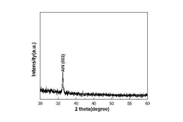
[0024] Dry the cleaned n-type Si (100) substrate and put it into a vacuum chamber. The distance between the substrate and the target is 60 mm. The target is Al (80 mm in diameter) with a purity of 99.999% and four A silicon wafer (length 10 mm, width 3 mm), the silicon wafer is symmetrically placed on the Al target, in-situ co-sputtering. Vacuum to 2.0×10 -4 Pa. The working gas in the sputtering process is high-purity nitrogen, the working pressure in the sputtering process is 1.5 Pa, and the substrate temperature is 370°C. Before the official sputtering, the sputtering power was adjusted to 300 W and the target was pre-sputtered for 20 min to remove impurities and oxide layers on the target surface. After the pre-sputtering was completed, the sputtering was started, and the sputtering time was 60 min.

[0025] From figure 1 It can be seen that the prepared film is AlN, and compared with the standard card, it can be seen that the film has a hexagonal wurtzite structure, a...

Embodiment 2

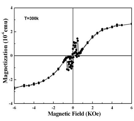
[0027]Dry the cleaned n-type Si (100) substrate and put it into a vacuum chamber. The distance between the substrate and the target is 60 mm. The target is Al (80 mm in diameter) with a purity of 99.999% and seven pieces A silicon wafer (length 10 mm, width 3 mm), the silicon wafer is symmetrically placed on the Al target, in-situ co-sputtering. Vacuum to 2.0×10 -4 Pa. The working gas in the sputtering process is high-purity nitrogen, the working pressure in the sputtering process is 1.5 Pa, and the substrate temperature is 370 °C. Before the official sputtering, the sputtering power was adjusted to 300 W and the target was pre-sputtered for 20 min to remove impurities and oxide layers on the target surface. After the pre-sputtering was completed, the sputtering was started, and the sputtering time was 60 min.

[0028] The M-H curve of the sample is obtained by superconducting quantum fluxmeter, such as image 3 As shown, it can be seen that the sample has obvious ferroma...

Embodiment 3

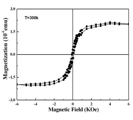
[0030] Dry the cleaned n-type Si (100) substrate and put it into a vacuum chamber. The distance between the substrate and the target is 60 mm. A silicon wafer (length 10 mm, width 3 mm), the silicon wafer is symmetrically placed on the Al target, in-situ co-sputtering. Vacuum to 2.0×10 -4 Pa. The working gas in the sputtering process is high-purity nitrogen, the working pressure in the sputtering process is 1.5 Pa, and the substrate temperature is 370 °C. Before the official sputtering, the sputtering power was adjusted to 300 W and the target was pre-sputtered for 20 min to remove impurities and oxide layers on the target surface. After the pre-sputtering was completed, the sputtering was started, and the sputtering time was 60 min.

[0031] The M-H curve of the sample is obtained by superconducting quantum fluxmeter, such as Figure 4 As shown, it can be seen that the sample has obvious ferromagnetic properties at room temperature, forming a standard hysteresis loop.


PUM

PropertyMeasurementUnit
purityaaaaaaaaaa
diameteraaaaaaaaaa

Abstract

The invention discloses a preparation method of an Si-doped AlN diluted magnetic semiconductor film, which uses high-purity nitrogen as work gas, high-purity Al targets and silicon wafers are adopted for in-situ co-sputtering, the background vacuum degree of a system is 10<-5>Pa to 10<-4> Pa, a substrate is n type Si(100), the distance from the targets and the substrate is 60mm, the sputtering power is 300W, the sputtering air pressure is 1.5Pa, and the substrate temperature is 370 DEG C, and the sputtering time is 60min. After the substrate is cleaned, and surface impurities are removed, the AlN diluted magnetic semiconductor film with different doping concentrations are obtained through changing the number of the doping silicon wafers. The method has the advantages that the preparation deposition velocity is high, the process is simple, and in addition, the diluted magnetic semiconductor film materials with the room temperature ferromagnetism and high Curie temperature can be obtained without any subsequent treatment, so the method has important study value and wide application prospects.

Description

technical field [0001] The invention belongs to the field of preparation of novel semiconductor spintronic device materials, and relates to an AlN-based dilute magnetic semiconductor thin film doped with non-magnetic main group elements and a preparation method thereof, in particular to a Si-doped AlN with room temperature ferromagnetism and high Curie temperature Preparation method of dilute magnetic semiconductor film. Background technique [0002] In recent years, dilute magnetic semiconductors (Diluted Magnetic Semiconductors, DMSs) have rapidly become a hot spot in the research of spintronics materials, because DMSs materials have both spin polarization and charge properties of electrons, and can avoid ferromagnetic metal-semiconductor The problem of conductivity mismatch at the interface, and secondly, DMSs are well compatible with existing semiconductor technologies when manufacturing devices. Therefore, it has broad application prospects in the fields of high-densit...

Claims


Application Information

Patent Timeline
Patent Type & Authority Applications(China)
IPC IPC(8): C23C14/35C23C14/06H01L43/12H01F41/18H01F10/193
Inventor 吴荣任银拴简基康潘东娄阳蒋小康李锦孙言飞任会会
Owner XINJIANG UNIVERSITY
Why Eureka
Try Eureka