Manufacturing method for distributed-feedback semiconductor laser with bar-shaped burying

A technology of distributed feedback and manufacturing methods, which is applied to semiconductor lasers, lasers, laser components, etc., and can solve problems such as complex processes and unreliability

Active Publication Date: 2012-03-07
WUHAN HUAGONG GENUINE OPTICS TECH
View PDF5 Cites 25 Cited by
  • Summary
  • Abstract
  • Description
  • Claims
  • Application Information

AI Technical Summary

Problems solved by technology

[0003] The manufacture of the BH structure requires multiple epitaxial growths, and the process i

Method used


Image

  • Manufacturing method for distributed-feedback semiconductor laser with bar-shaped burying
  • Manufacturing method for distributed-feedback semiconductor laser with bar-shaped burying
  • Manufacturing method for distributed-feedback semiconductor laser with bar-shaped burying

Examples


Embodiment Construction

[0028] In order to facilitate a further understanding of the method and the achieved effects of the present invention, the preferred embodiments are described in detail below in conjunction with the drawings.

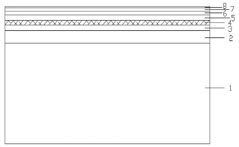
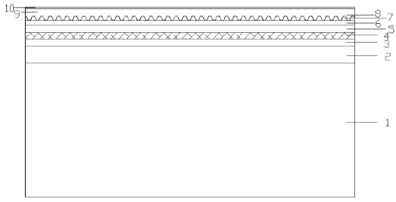
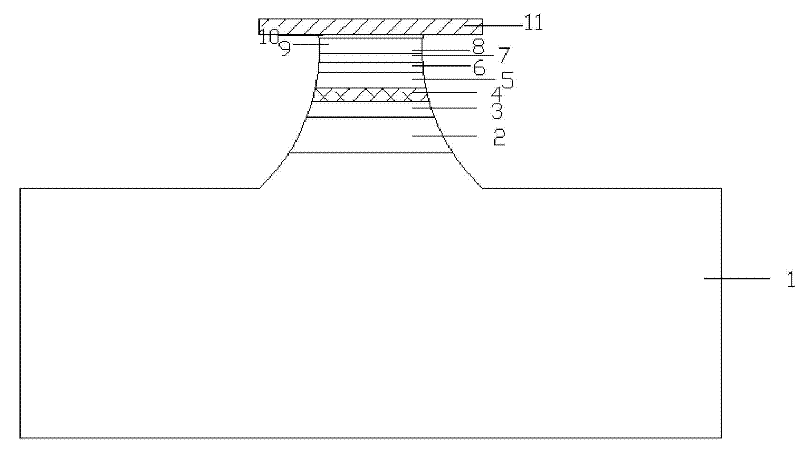
[0029] Please refer to Figure 1 to Figure 6 As shown, the present invention is the multi-layer heterostructure / strained multi-quantum well epitaxial layer required for the epitaxial growth of the laser on the N-type indium phosphide (InP) substrate, which is the primary epitaxial wafer; and then on the basis of the primary epitaxial wafer Fabrication of distributed feedback Bragg gratings, fabrication of ridge strip structures by dry etching and two-step wet etching, and implementation of SiO 2 (Silicon dioxide) cantilever; after special treatment by MOVCD (Metal-organic Chemical Vapor Deposition, metal organic compound chemical vapor deposition), ridge strip burial, etc.

[0030] Below with reference to accompanying drawing, introduce each step of method of the prese...


PUM

PropertyMeasurementUnit
Wavelengthaaaaaaaaaa
Thicknessaaaaaaaaaa
Thicknessaaaaaaaaaa

Abstract

The invention discloses a manufacturing method for a distributed-feedback semiconductor laser with bar-shaped burying. According to the method, primary epitaxy is carried out to form a primary epitaxial wafer; a single-beam spherical light mode is utilized to manufacture a distributed-feedback bragg grating with a gradient wavelength; a metal-organic chemical vapor deposition technology is utilized to carry out grating burying; a mode of combination of reactive ion etching and a two-step wet etching is used to manufacture a ridged bar; the metal-organic chemical vapor deposition (MOVCD) technology is used to carry out high-temperature meltback and then bar-shaped burying is carried out by a rapid growth mode; a SiO2 buried bar and a InGaAsP protective layer are removed and P type InP cover coat and a P+ In GaAs contact layer is grown; a large dual-channel structure is manufactured, a SiO2 insulated dielectric film is deposited, a P side electrode is manufactured, a substrate is thinned, an N side electrode is manufactured, an optical film is evaporated and plated on an end surface, and a laser chip is manufactured finally. According to the manufacturing method provided in the invention, the manufactured laser has characteristics of low threshold, low resistance, wide and stable working temperature range, high reliability and high yield and the like.

Description

technical field [0001] The invention relates to a manufacturing method of an optoelectronic device for optical communication, in particular to a manufacturing method of a strip-shaped buried distribution feedback semiconductor laser with an optical wavelength of 1490nm. Background technique [0002] Semiconductor lasers carry out carrier confinement and optical field confinement from the side, and there are mainly two structures: ridge waveguide (RWG) and buried heterojunction (BH). Due to the large refractive index difference of the lateral material, the BH structure forms a strong refractive index guide, which can better confine the carriers and the light field, so it has the advantages of low threshold current, wide operating temperature range and small far-field divergence angle. Features; at the same time, the BH structure has the characteristics of small size of the active layer (its width should be less than 1.6um), and has a stable side mode control effect. [0003]...

Claims


Application Information

Patent Timeline
IPC IPC(8): H01S5/12H01S5/343H01S5/223
Inventor 许海明唐琦刘建军
Owner WUHAN HUAGONG GENUINE OPTICS TECH
Why Eureka
Try Eureka