Capacitance-free dynamic random access memory structure and preparation method thereof

A dynamic random, non-capacitive technology, applied in semiconductor/solid-state device manufacturing, circuits, electrical components, etc., can solve problems such as reducing the probability of impact ionization, disturbance of gate dielectric data, and reduction of channel threshold voltage near the drain region. Achieve the effects of high-density three-dimensional process integration, suppression of gate dielectric degradation, and suppression of short channel effects

Active Publication Date: 2012-03-14
宁夏储芯科技有限公司
View PDF7 Cites 16 Cited by
  • Summary
  • Abstract
  • Description
  • Claims
  • Application Information

AI Technical Summary

Problems solved by technology

In this programming mode, the drain terminal voltage is greater than the gate voltage due to the high impact ionization rate, such as Vg=0.5V, Vd=2V, Vs=0V, so the generated holes are still moving to the substrate. Part of it moves to the gate dielectric, thereby generating interface traps and oxide layer traps near the drain junction. With multiple programming and erasing operations, the holes in the gate dielectric will further accumulate, resulting in the threshold voltage of the channel near the drain region Reduced, thus causing information disturbance or error when data is read
For programming mode with tunneling BTBT ( figure 2 b), usually the source terminal is floating, and the drain terminal voltage is much higher than the gate voltage, such as Vg=0V, Vd=4V. In this mode, electrons will move to th

Method used


Image

  • Capacitance-free dynamic random access memory structure and preparation method thereof
  • Capacitance-free dynamic random access memory structure and preparation method thereof
  • Capacitance-free dynamic random access memory structure and preparation method thereof

Examples


Embodiment Construction

[0039] In order to make the object, technical solution and advantages of the present invention clearer, the present invention will be described in further detail below in conjunction with specific embodiments and with reference to the accompanying drawings.

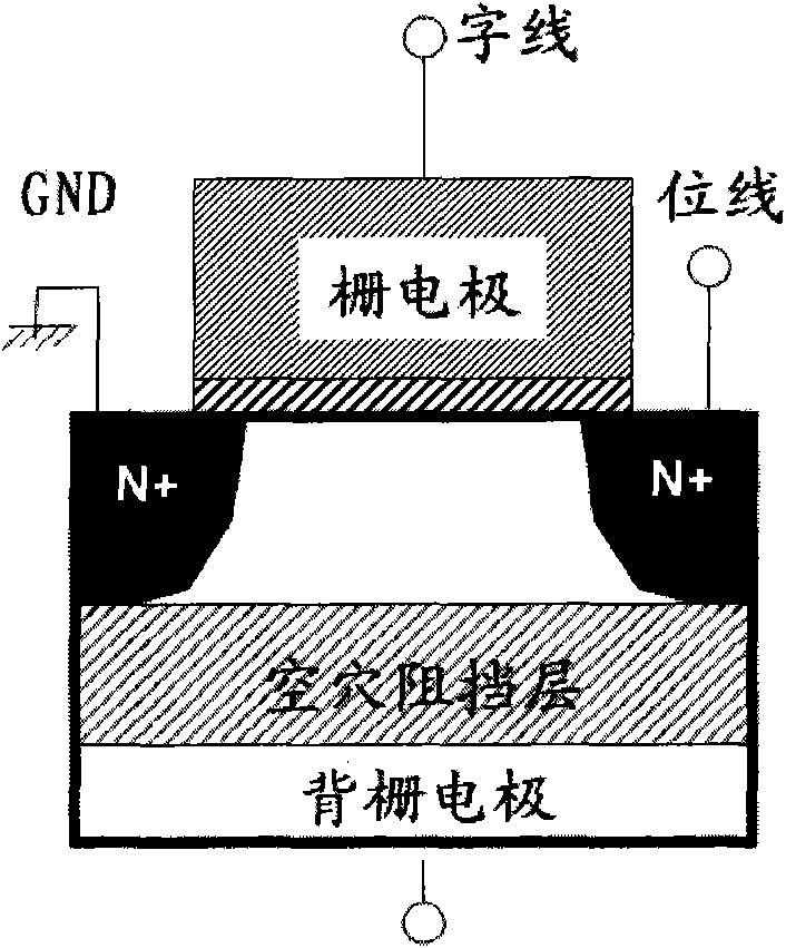
[0040] figure 1 is a schematic diagram of a conventional non-capacitance floating body memory cell structure, holes will be stored in the area close to the hole blocking layer. Here the hole blocking layer can be made of SiO 2 It can also be realized by using n-doped Si, or even by using SiGe, SiC, etc. At the same time, the substrate or the back gate can be grounded, and negative voltage bias can also be realized.

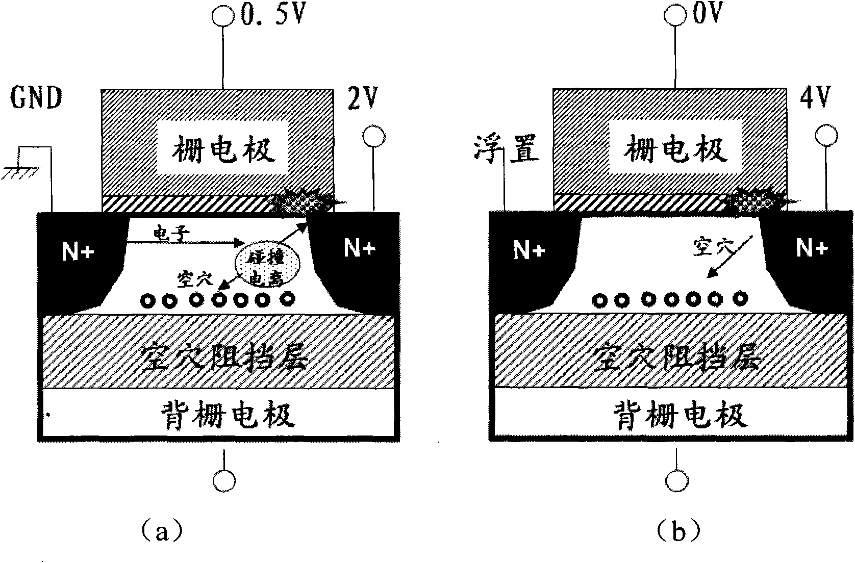
[0041] figure 2 It is a schematic diagram of two programming modes of a conventional floating body memory unit. In channel hot electron programming mode ( figure 2 a) Apply a large positive voltage such as 2V to the drain, and apply a transistor turn-on voltage such as 0.5V to the gate. The source vol...


PUM


Abstract

The invention discloses a capacitance-free dynamic random access memory structure and a preparation method thereof. Under the premise that the capacitance-free dynamic random access memory structure meets high voltage leakage requirements for a high impact ionization rate, the electrical thickness of a gate medium in a source drain junction area is increased via adoption of different gate medium materials or gate medium thicknesses near the area, an electric field in the vertical direction is reduced effectively. Meanwhile, a thin oxidation layer or a high K material is adopted in the central area of a channel, the gate control capability is improved, and the short channel effect is inhibited. By adopting the structure, the degradation of the gate medium can be inhibited effectively, the reliability (durability) of a storage unit can be improved, the scaling-down of a device can be facilitated, and the complex process for the capacitance structure in the conventional 1T1C structure can be avoided completely in the capacitance-free structure. The adopted manufacturing process is completely compatible with the conventional logic process, and the high-density three-dimensional process integration can also be facilitated.

Description

technical field [0001] The invention relates to the technical fields of microelectronics manufacturing and memory, in particular to a highly reliable non-capacitive dynamic random access memory structure and a preparation method thereof. Background technique [0002] Microelectronics products are mainly divided into two categories: logic devices and memory devices. As an important part of storage devices, dynamic random access memory (DRAM) can provide high-speed data read and write operations, but the stored information is easily lost in the event of power failure, so it is called volatile semiconductor memory. In computer systems, DRAMs are generally placed between high-speed microprocessors and low-speed non-volatile memories, and are used to match high-speed data processing and low-speed data access. With the continuous development of information technology, the development of high-speed and high-density DRAM has become an important direction of storage technology resea...

Claims


Application Information

Patent Timeline
IPC IPC(8): H01L27/108H01L29/423H01L29/51H01L21/8242
Inventor 霍宗亮刘明
Owner 宁夏储芯科技有限公司
Why Eureka
Try Eureka