Method for preparing primary circuit by jet-printing metal conductive printing ink by virtue of laser or microwave processing

A primary circuit, metal conductive technology, applied in the post-processing, printing and other directions of printing, can solve problems such as difficult application, difficult operation, high price, etc., to achieve a wide range of substrates or films, improve conductivity, and increase the effect of adhesion

Inactive Publication Date: 2012-04-04
INST OF CHEM CHINESE ACAD OF SCI
View PDF9 Cites 6 Cited by
  • Summary
  • Abstract
  • Description
  • Claims
  • Application Information

AI Technical Summary

Problems solved by technology

The above temperature-controlled sintering method can only be applied to high-temperature-resistant printing materials such as glass, ceramics, metal, and polyimide, and it is still difficult to apply to printing films with low glass transition temperatures such as PET, PVC, PC, and paper.
Literature (Chem.Phys.Lett.2007, 441, 305-308.) has reported the use of solvents such as methanol to clean the printed circuit to wash off the organic substances in the circuit. This method improves the electrical conductivity of the printed circuit, but only uses Cleaning circuits with organic solvents is not suitable for large-scale preparation, and it also increases the solvent resistance requirements of the printing plate, and at the same time increases the pressure of organic solvents on environmental pollution
In 2008, Finnish scientist Mark L. Allen et al. (VTT Technical Research Center of Finland, Nanotechnology, 19 (2008) 175201 (4pp)) directly applied voltage across the primary printed circuit, using current and thermal resistance to melt Metal particles also significantly improve the conductivity of the primary printed circuit, but the direct voltage application method is not easy to operate, high voltage is easy to break down the printing plate / film, and high voltage is not safe
[0007] In 2009, German and Dutch scientists headed by Ulrich S.Schubert (J.Mater.Chem., 2009, 19, 3384-3388) used plasma to process the primary printed circuit, and also obtained a circuit with high conductivity , but the requirements of plasma on vacuum degree and high price determine that it can only stay at the laboratory level

Method used


Image

  • Method for preparing primary circuit by jet-printing metal conductive printing ink by virtue of laser or microwave processing
  • Method for preparing primary circuit by jet-printing metal conductive printing ink by virtue of laser or microwave processing

Examples


Embodiment 1

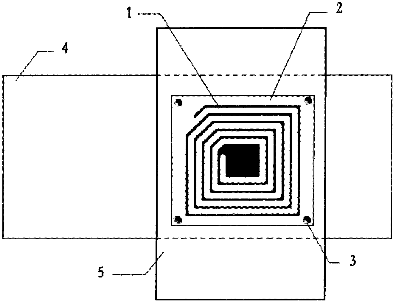
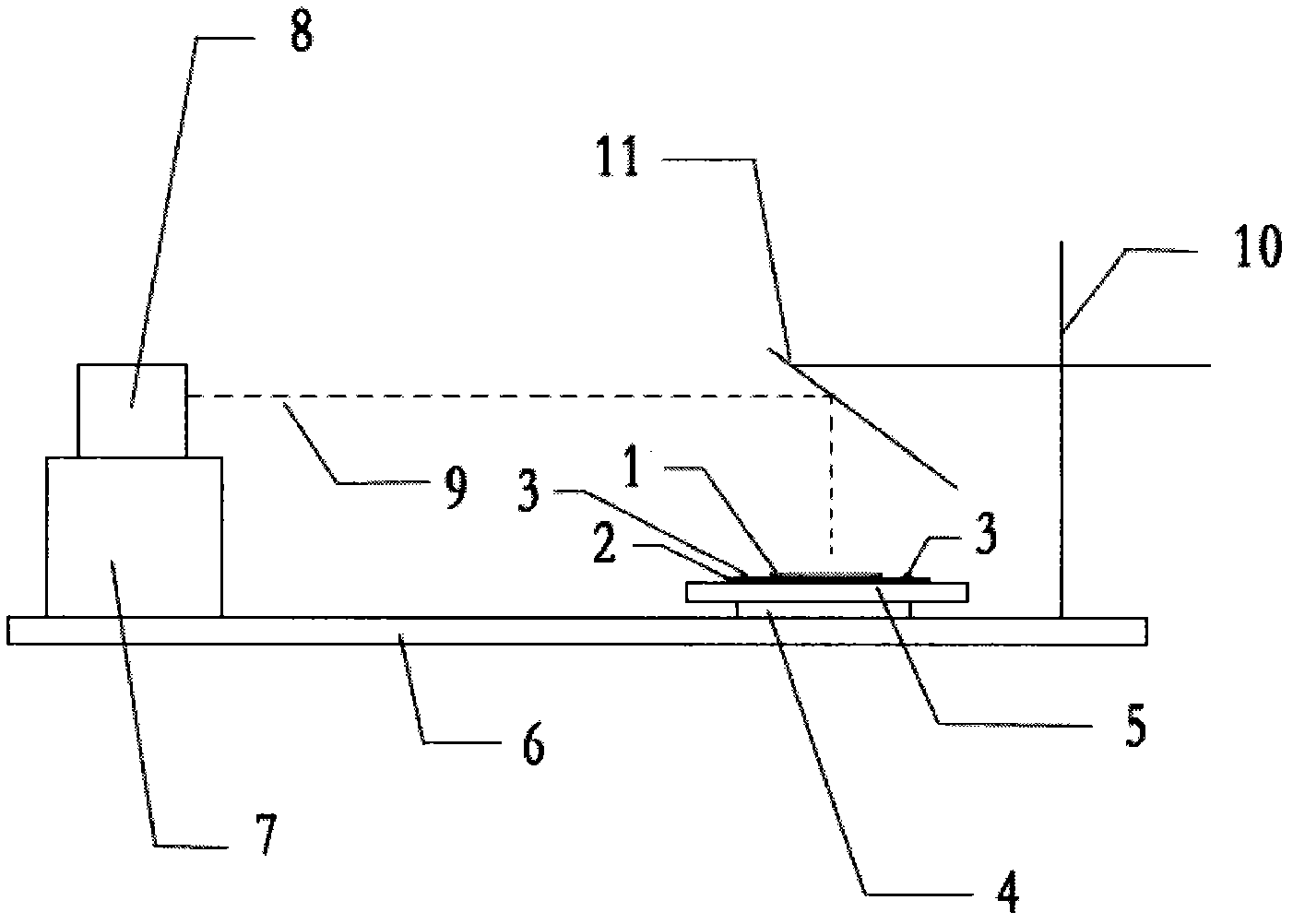
[0057] See figure 2 The shown device for continuous scanning exposure sintering primary circuit: a base 7 is installed on one side of an optical table 6, and a laser 8 is installed on the base 7; The stage of the X-direction electric translation stage 4 and the Y-direction electric translation stage 5, on which the substrate / film 2 carrying the primary circuit 1 is placed, and the substrate / film 2 carrying the primary circuit 1 can be Fixed on the object stage capable of electric translation in the X direction and the Y direction through the fixing buckle 3; a support frame 10 is installed on the optical table 6 on the side of the object stage; a mirror 11 is installed on the support frame 10, And the reflector 11 is located above the stage, and can make the laser beam 9 emitted by the laser head 8 be perpendicular to the stage after being reflected by the reflector. The method of using the device for continuous scanning exposure sintering primary circuit is as follows:

[...

Embodiment 2

[0062] 1) According to the preset circuit pattern by the inkjet printer, the metallic silver conductive ink (NanoMas Technologies, Inc., NMTI NanoGold Inks (NTG05)) with a mass fraction of 20% and a particle size of 20nm was electrostatically printed on the On the polycarbonate film, the primary circuit with a film thickness of 0.4 μm formed by the above-mentioned conductive ink is obtained on the polycarbonate film, and the PET polyester film carrying the primary circuit is fixed on the stage;

[0063] 2) Position the laser head at the starting point of the primary circuit in step 1), use a computer program to control the laser beam (wavelength: 432nm; power: 1w) emitted by the laser head, follow step 1) when the inkjet printer is printing the circuit pattern The running track moves, and the moving speed of the laser beam emitted by the laser head is 30cm / s; the laser beam emitted by the laser head only selects the primary circuit on the polycarbonate film on the stage 1) Sca...

Embodiment 3

[0067]1) According to the preset circuit pattern by the inkjet printer, the metal copper conductive ink (NovaCentrix. On the imide plate, obtain a primary circuit with a film thickness of 40 μm formed by the above-mentioned conductive ink on the polyimide plate, and fix the polyimide plate with the primary circuit on the stage;

[0068] 2) Position the laser head at the starting point of the primary circuit in step 1, use a computer program to control the laser beam (wavelength: 1064nm; power: 1.5w) emitted by the laser head, and the moving speed of the laser beam emitted by the laser head is 50cm / s, the spot where the laser beam emitted by the laser head falls on the primary circuit is obtained by vertically and directly irradiating the primary circuit with the laser beam emitted by the laser head;

[0069] Use the laser beam emitted by the laser head to continuously scan the polyimide plate on the stage 1) carrying the primary circuit, control the laser beam emitted by the ...


PUM


Abstract

The invention belongs to an ink jet printing (jet printing for short) circuit technology, relating to a primary circuit or microwave processing primary circuit prepared by jet-printing metal conductive printing ink by utilizing a laser sintering method, and aiming at degrading organic components in the printing ink and improving conductive properties of the obtained jet printing circuit. In the method for preparing the primary circuit by printing the metal conductive printing ink by virtue of laser or microwave processing, laser continuous scanning, exposing and sintering, selective scanning, exposing and sintering, overall exposing and sintering or selective exposing and sintering are carried out on the primary circuit prepared by jet-printing the metal conductive printing ink, or the primary circuit prepared by jet-printing the metal conductive printing ink is sintered by virtue of microwave processing, so as to improve electric conductivity of the jet-printed circuit; the jet-printed primary circuit is processed by utilizing the laser with high speed, high efficiency and positioning accuracy, thus being applicable to extensive printing boards or films; and requirements on material and shape (hard board or film) of the printing board or film are not strict, and thus the method is applicable to automation.

Description

technical field [0001] The invention belongs to inkjet printing (jet printing for short) circuit technology, relates to the post-processing method of the primary circuit prepared by spray printing metal conductive ink, especially relates to the primary circuit prepared by spray printing metal conductive ink by laser sintering method or microwave treatment Primary circuit to degrade the organic components in the ink and improve the electrical conductivity of the resulting jet printed circuit. Background technique [0002] Inkjet printing (referred to as inkjet printing) circuit technology is a cutting-edge advanced circuit board manufacturing technology. It is a product of computer-aided control printing technology. Printing plate / film, especially flexible printing film; its working process is to first input the pattern information stored in the computer into the inkjet printer, and under the control of the computer, the nozzle of the inkjet printer sprays conductive ink (ele...

Claims


Application Information

Patent Timeline
Patent Type & Authority Applications(China)
IPC IPC(8): B41M7/00
Inventor 张志良安粒张兴业宋延林
Owner INST OF CHEM CHINESE ACAD OF SCI
Why Eureka
Try Eureka