
Method for manufacturing non-refrigerant thermal infrared detector based on black silicon material

A non-cooling and thermal infrared technology, which is applied in the coating process of metal materials, the process for producing decorative surface effects, and the manufacture of microstructure devices, etc. It can solve the problems that infrared radiation cannot directly convert electrical signals and does not have much meaning , to achieve great application prospects and research value, low cost and high sensitivity

Inactive Publication Date: 2012-05-02
INST OF SEMICONDUCTORS - CHINESE ACAD OF SCI
View PDF5 Cites 19 Cited by
  • Summary
  • Abstract
  • Description
  • Claims
  • Application Information

AI Technical Summary

Problems solved by technology

[0004] However, studies have found that the absorption of medium and long-wave infrared light by black silicon materials is mainly caused by defect energy levels. These defect energy levels will also become carrier recombination centers while absorbing infrared radiation, so that the absorbed infrared radiation cannot be directly absorbed. Converted into electrical signals, but converted into thermal energy of materials, so the high infrared radiation absorption characteristics of black silicon materials are not very meaningful for the preparation of photon infrared detectors

Method used


Image

  • Method for manufacturing non-refrigerant thermal infrared detector based on black silicon material
  • Method for manufacturing non-refrigerant thermal infrared detector based on black silicon material
  • Method for manufacturing non-refrigerant thermal infrared detector based on black silicon material

Examples


Embodiment Construction

[0030] In order to make the object, technical solution and advantages of the present invention clearer, the present invention will be described in further detail below in conjunction with specific embodiments and with reference to the accompanying drawings.

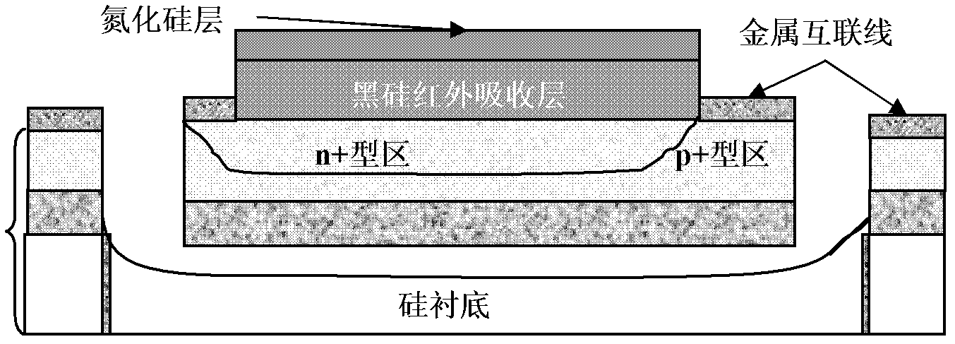
[0031] What attracts people's attention is that black silicon has an absorption effect similar to that of a black body in the full solar spectrum range, and this material is based on silicon and is also compatible with the currently commonly used CMOS and SOI-CMOS processes. However, current research has found that most of the absorption of infrared radiation by black silicon materials is caused by defect energy levels, and it is difficult to directly convert this part of the absorption into photocurrent. According to the characteristics of high infrared radiation absorption and low infrared photogenerated carrier output of the black silicon material, the invention combines the black silicon material as an infrared radiati...


PUM


Abstract

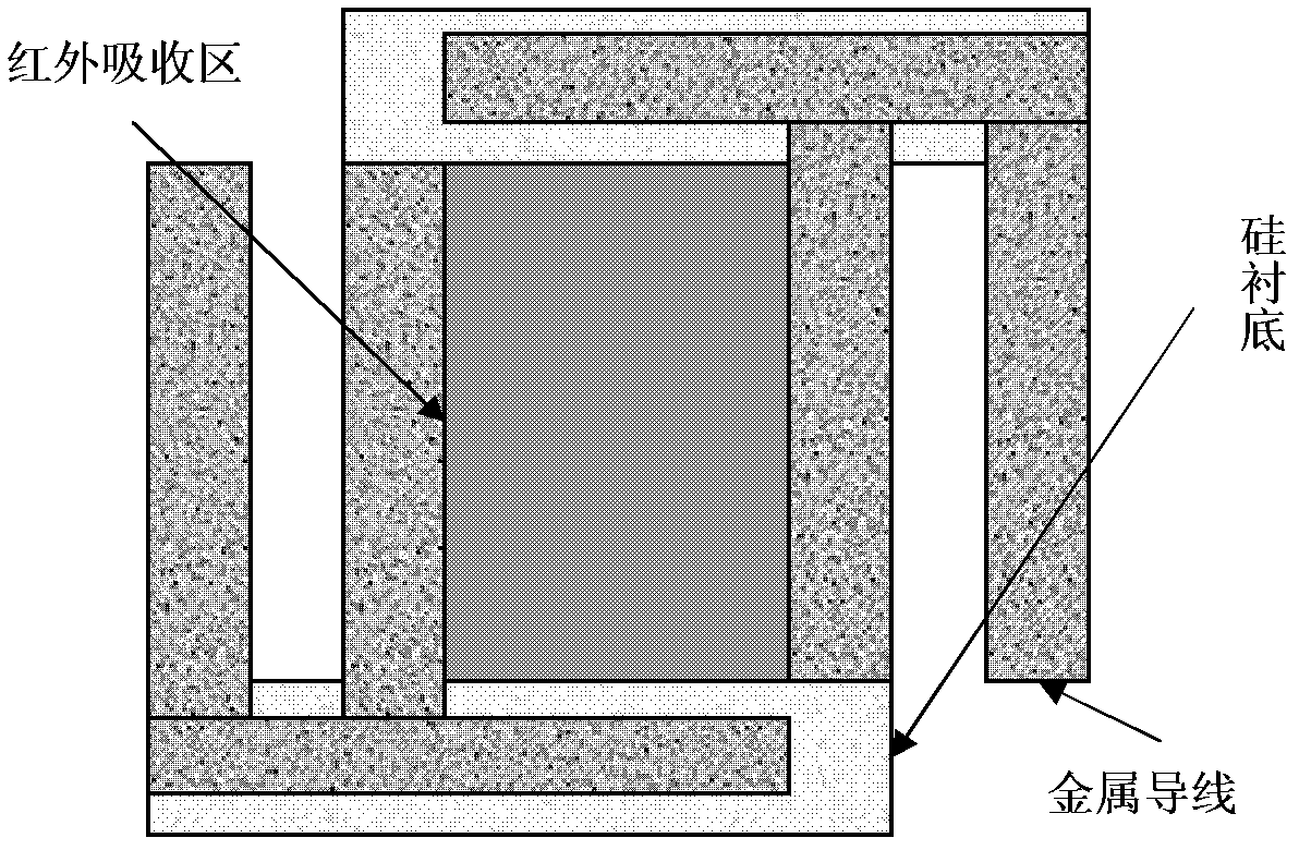
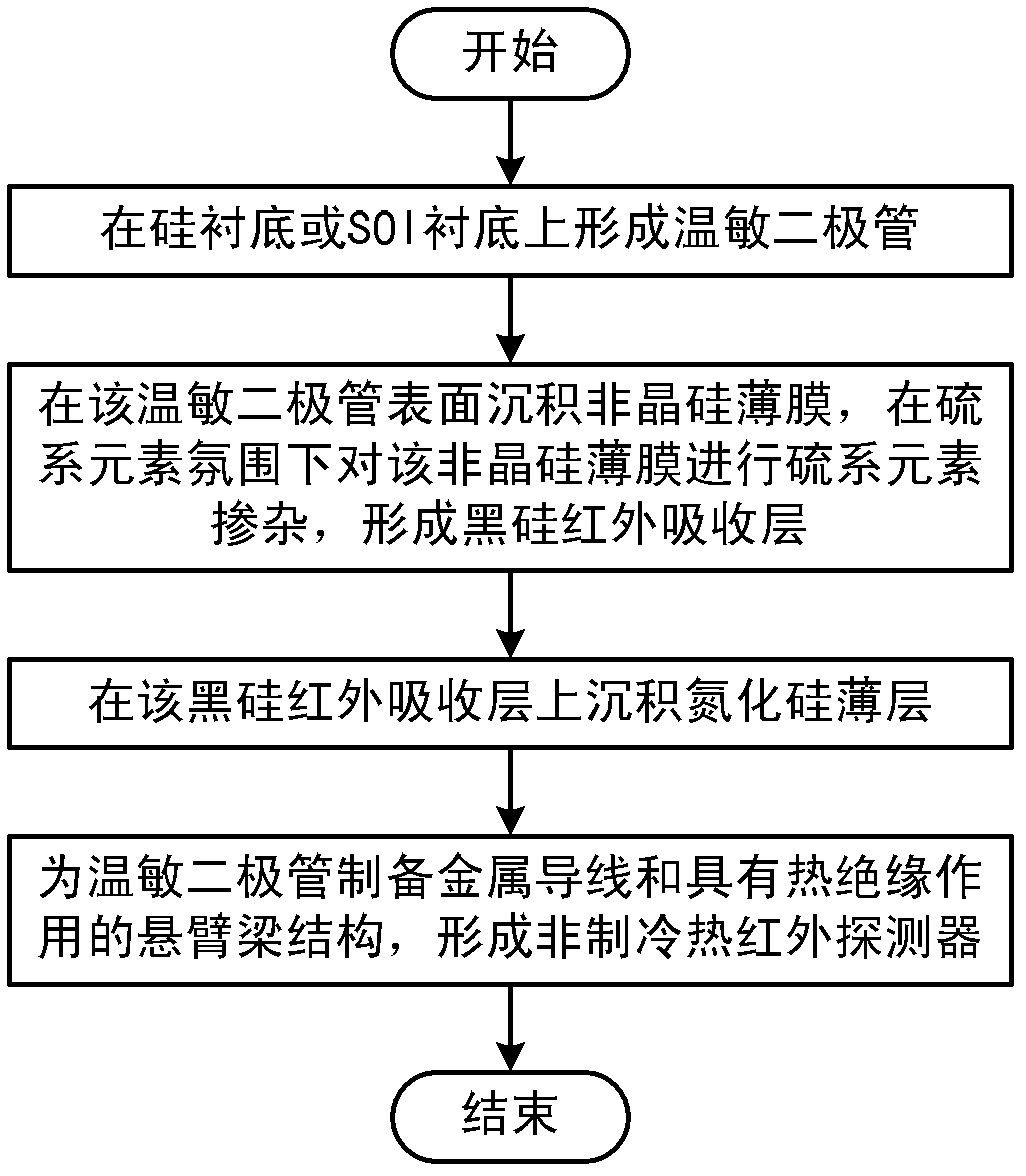
The invention discloses a method for manufacturing a non-refrigerant thermal infrared detector based on a black silicon material. The method comprises the following steps of: forming a thermosensitive diode on a silicon substrate or a silicon-on-insulator (SOI) substrate; depositing an amorphous silicon film on the surface of the thermosensitive diode, and performing sulfur element doping on the amorphous silicon film in an ultrafast laser irradiation mode or sulfur element ion implantation and ultrafast laser irradiation modes in the presence of sulfur elements to form a black silicon infrared absorbing layer; depositing a silicon nitride thin layer on the black silicon infrared absorbing layer to be used as a surface passivation layer; and preparing a metal conducting wire and a cantilever beam structure with a thermal insulation effect for the thermosensitive diode to form the non-refrigerant thermal infrared detector. In the method, the characteristics that the black silicon material has high infrared irradiation absorbability and is compatible with a micro-electronic processing process easily are fully utilized, and the manufactured thermal infrared detector has the advantages of high sensitivity and low cost and is easy to manufacture through an SOI complementary metal oxide semiconductor (CMOS) process and a CMOS process.

Description

technical field [0001] The invention relates to the technical field of uncooled thermal infrared detectors, in particular to a method for preparing an uncooled thermal infrared detector based on black silicon material. Background technique [0002] The essence of an uncooled infrared detector array is a MEMS device integrated with a thermal infrared detector pixel array. The uncooled MEMS infrared detector integrated infrared radiation absorption layer on the silicon temperature sensitive diode is one of the research hotspots in the field of uncooled infrared detector [1][6][7] . [0003] Since the advent of black silicon material, it has been close to the absorption effect of black body in the whole solar spectrum range. [2] And it has received widespread attention. In 2006, T.G.Kim et al. from Harvard University in the United States reported a super-infrared absorbing material that is supersaturated with sulfur on a silicon substrate to form a sub-band gap. [3] . In 20...

Claims


Application Information

Patent Timeline
IPC IPC(8): B81C1/00
Inventor 韩培德李辛毅毛雪胡少旭王帅范玉杰
Owner INST OF SEMICONDUCTORS - CHINESE ACAD OF SCI
Learn More