Method for increasing writing speed of floating body effect storage unit and semiconductor device

A storage unit and writing speed technology, applied in semiconductor/solid-state device manufacturing, electrical components, transistors, etc., can solve problems such as leakage and need to be improved, reduce leakage speed, improve writing speed, and increase substrate current Effect

Active Publication Date: 2014-01-08
SHANGHAI HUALI MICROELECTRONICS CORP
View PDF5 Cites 0 Cited by
  • Summary
  • Abstract
  • Description
  • Claims
  • Application Information

AI Technical Summary

Problems solved by technology

[0005] When the floating body effect memory cell is writing "1", the carriers will accumulate in the substrate while slowly leaking from the source. The inventor believes that the writing speed of the floating body effect memory cell ("1") has yet to be reached improve

Method used


Image

  • Method for increasing writing speed of floating body effect storage unit and semiconductor device
  • Method for increasing writing speed of floating body effect storage unit and semiconductor device
  • Method for increasing writing speed of floating body effect storage unit and semiconductor device

Examples


Embodiment Construction

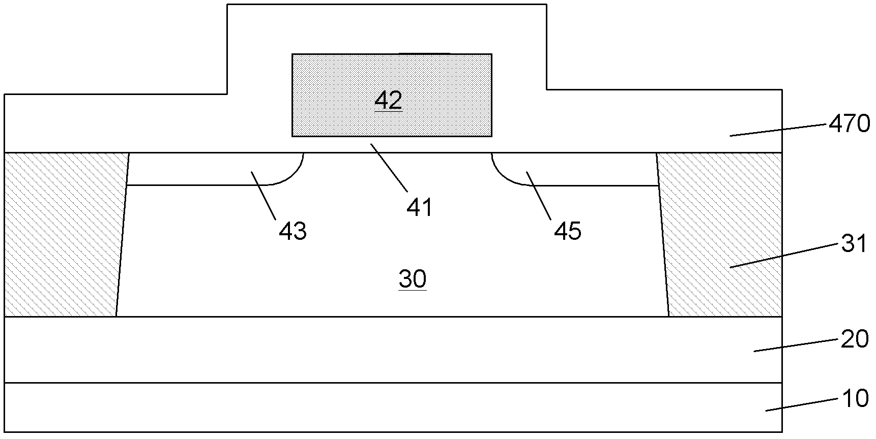
[0018] In the usual process, the sidewall formation (deposition and etching) process of the floating body effect memory cell is as follows: Figure 2A-2C shown.

[0019] First, the sidewall material is deposited, and the cross-section of the device after deposition is as follows Figure 2A shown. The floating body effect memory unit in the figure comprises bottom silicon 10, and described bottom silicon 10 is silicon-on-insulator for example; Formed on bottom silicon 10 Buried oxide layer 20; Formed on the substrate 30 of buried oxide layer 20, described The substrate 30 can be a silicon substrate, of course, in some occasions, a germanium substrate, a silicon germanium substrate or other semiconductor materials can also be applied; the shallow trench isolation groove 31 (shallow trench isolation, That is, STI), used to isolate each floating body effect memory cell; a gate oxide layer 41 and a gate 42 formed sequentially on the substrate 30, and a channel in the substrate 30...


PUM


Abstract

The invention provides a method for increasing the writing speed of a floating body effect storage unit and an intermediate transitional semiconductor device, belonging to the technical field of semiconductor manufacturing. The core of the invention is as follows: when a side wall material is deposited, an included angle between the introduction direction of reactant plasma and the surface of a substrate in a source position is less than 90 DEG, and an included angle between the introduction direction of the reactant plasma and the surface of a substrate in a drain position is more than 90 DEG; the side wall material is etched, side walls are formed at two sides of a gate, and the width of the side wall close to a source is more than that of the side wall close to a drain; taking the side walls as masks, heavy doping and annealing processes are carried out to form the source and the drain, and a distance between doped ions of the drain and a channel is closer and a distance between doped ions of the source and the channel as well as the substrate is further. According to the invention, on the one hand, the longitudinal electric field in the drain channel is enhanced and the substrate current is increased, on the other hand, the leakage speed of accumulated carriers from the source is reduced, and therefore the writing speed of the floating body effect storage unit is increased.

Description

technical field [0001] The invention relates to the technical field of semiconductor manufacturing, in particular to a manufacturing method capable of increasing the writing speed of a floating body effect memory unit and an intermediate transition semiconductor device. Background technique [0002] The development of embedded dynamic storage technology has made large-capacity dynamic random access memory (Dynamic Random Access Memory, DRAM) very common in current System on a Chip (SoC). Large-capacity embedded DRAM brings SoC benefits such as improved bandwidth and reduced power consumption that can only be achieved by using embedded technology. In addition to transistors, each storage unit of traditional embedded dynamic random access memory (embbeded Dynamic Random Access Memory, eDRAM) also needs a deep trench capacitor structure. The deep trench of the capacitor makes the height of the storage unit larger than its width. Much larger, causing manufacturing process diffi...

Claims


Application Information

Patent Timeline
Patent Type & Authority Patents(China)
IPC IPC(8): H01L21/8242H01L27/108
Inventor 俞柳江周军
Owner SHANGHAI HUALI MICROELECTRONICS CORP
Why Eureka
Try Eureka