Quantum well infrared focal plane photosensitive element chip with grating in bottom coupling mode and preparation method thereof

A technology of well infrared focus and coupling grating, which is applied in the field of bottom coupled grating quantum well infrared focus plane photosensitive element chip and its preparation, achieving the effect of novel and unique structure, avoiding manufacturing process and simple method

Inactive Publication Date: 2012-05-02
HENAN POLYTECHNIC UNIV
View PDF2 Cites 7 Cited by
  • Summary
  • Abstract
  • Description
  • Claims
  • Application Information

AI Technical Summary

Problems solved by technology

[0005] In view of the above situation, in order to overcome the defects of the prior art, the object of the present invention is to provide a bottom-coupled grating quantum well infrared focal plane photosensitive element chip and its preparation method, which can effectively solve the problem of improving the grating coupling mode of the chip and simplify the focal plane photosensitive element chip. The problem of improving the coupling efficiency of gratings in the fabrication process of meta-chips

Method used


Image

  • Quantum well infrared focal plane photosensitive element chip with grating in bottom coupling mode and preparation method thereof
  • Quantum well infrared focal plane photosensitive element chip with grating in bottom coupling mode and preparation method thereof
  • Quantum well infrared focal plane photosensitive element chip with grating in bottom coupling mode and preparation method thereof

Examples


Embodiment Construction

[0013] The specific implementation manners of the present invention will be described in detail below in conjunction with the accompanying drawings.

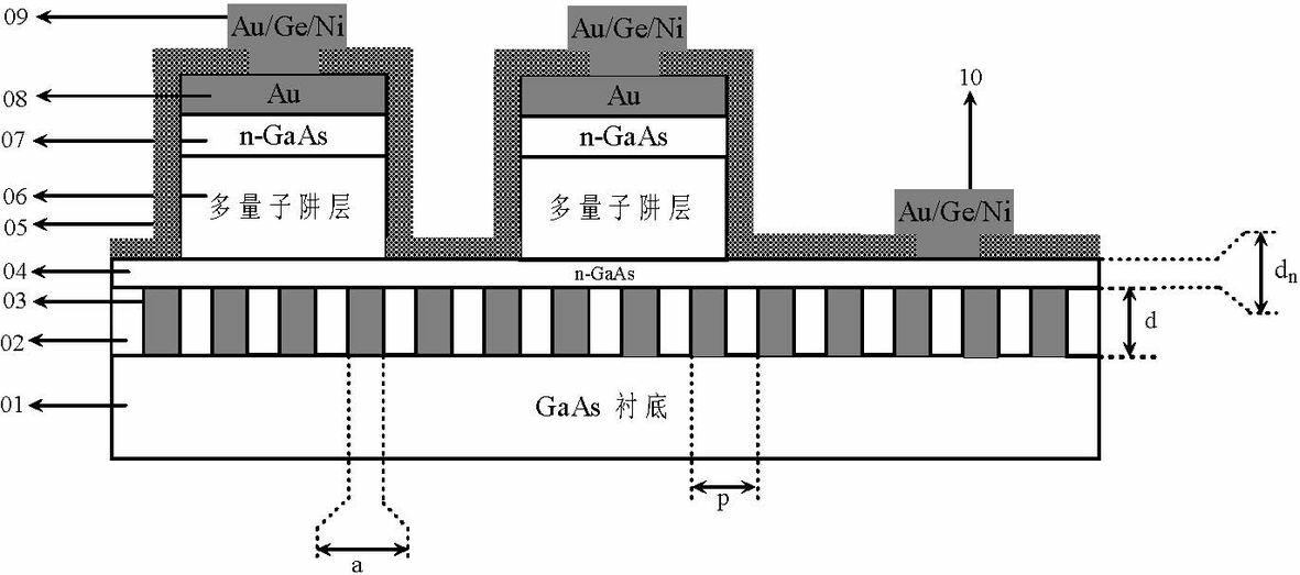
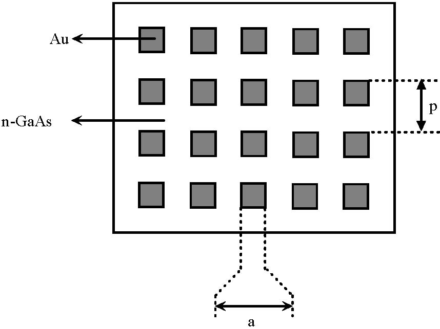
[0014] Depend on figure 1 Given, the photosensitive element chip of the present invention is composed of several parts from bottom to top:

[0015] On the gallium arsenide substrate 01, there is a transmission grating composed of n-type gallium arsenide 02 and gold 03 alternately and periodically arranged. There is a GaAs / AlGaAs multi-quantum well layer 06, an n-type gallium arsenide upper contact layer 07 on the GaAs / AlGaAs multi-quantum well layer, a gold (Au) reflective layer 08 on the n-type gallium arsenide upper contact layer, gold ( On the Au) reflective layer, there is a gold / germanium / nickel (Au / Ge / Ni) alloy upper electrode 09, and one end of the n-type gallium arsenide lower contact layer 04 has a gold / germanium / nickel alloy common lower electrode 10, n-type arsenic Gallium oxide lower contact layer, GaAs / AlGaAs mult...


PUM


Abstract

The invention relates to a quantum well infrared focal plane photosensitive element chip with a grating in a bottom coupling mode and a preparation method thereof; therefore, problems that a manufacturing process of a focal plane photosensitive element chip is simplified and grating coupling efficiency is improved can be effectively solved. The chip is characterized in that: a transmission grating that is formed by n type gallium arsenide and Au in an alternative and periodic arrangement is formed on a gallium arsenide substrate; a lower contact layer is arranged on the transmission grating; multi-quantum well layers are formed on the lower contact layer; upper contact layers are formed on the multi-quantum well layers; Au reflecting layers are arranged on the upper contact layers; alloy upper electrodes are arranged on the Au reflecting layers; an alloy common lower electrode is formed on one end of the lower contact layer; and silica passivation layers are formed at two sides of thelower contact layer, the multi-quantum well layers, the upper contact layers, the Au reflecting layers, the alloy upper electrodes and the alloy upper electrodes. According to the preparation method,a wafer bonding technology and a conventional semiconductor technology are employed to place a transmission grating at the bottom of multi-quantum well layers, so that an integrated structure is formed. According to the invention, the structure is novel and unique; optical coupling efficiency is improved; and the manufacturing technology and the method are simple.

Description

technical field [0001] The invention relates to the field of semiconductor optoelectronic devices, in particular to a bottom coupling grating quantum well infrared focal plane photosensitive element chip and a preparation method thereof. Background technique [0002] GaAs / AlGaAs quantum well infrared detector (Quantum Well Infrared Photodetector, referred to as QWIP) with its mature material growth and preparation process, easy to integrate large area array, good stability, good device uniformity, low cost, easy to achieve two-color and multi-color The advantages of focal plane devices and radiation resistance have broad application prospects in the fields of national defense detection, forest fire prevention, industrial monitoring, and medical care. It has become a research hotspot in the field of infrared detection in recent years. [0003] However, according to the selection rule of the quantum transition, the QWIP device is prohibitive to normal incident infrared light. ...

Claims


Application Information

Patent Timeline
Patent Type & Authority Applications(China)
IPC IPC(8): H01L31/101H01L31/0352H01L31/18
CPCY02P70/50
Inventor 王国东王允建李端谢贝贝杨莹丽王素玲
Owner HENAN POLYTECHNIC UNIV
Why Eureka
Try Eureka