Sb2Tex-SiO2 nano composite phase change material used on phase change memory and preparation method of Sb2Tex-SiO2 nano composite phase change material
A phase change memory and phase change material technology, applied in the field of Sb2Tex-SiO2 nanocomposite phase change material and preparation, can solve the problems of low crystallization temperature, poor thermal stability, hindering the application of phase change memory, etc.
- Summary
- Abstract
- Description
- Claims
- Application Information
AI Technical Summary
Problems solved by technology
Method used
Image
Examples
Embodiment 1
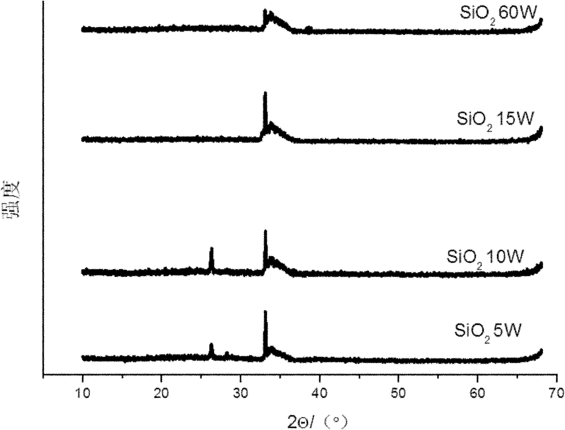
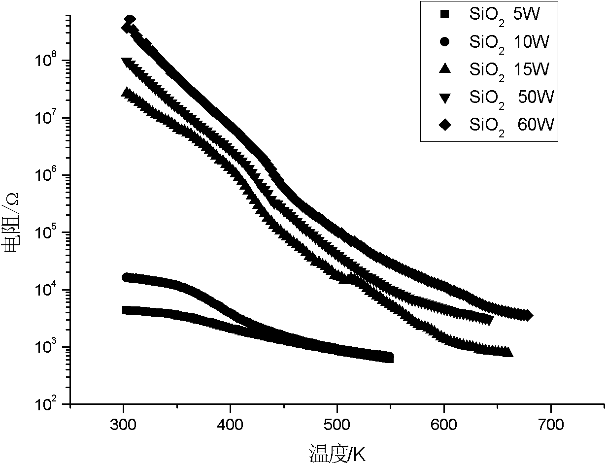
[0029] The nanocomposite phase change material in this embodiment can adopt Sb 2 Te 3 target and SiO 2 Prepared by target co-sputtering method. The specific preparation conditions are as follows: Ar gas with a purity of 99.999% is introduced simultaneously during the co-sputtering process. Sb 2 Te 3 target and SiO 2 Targets use RF power, Sb 2 Te 3 The power of the target is set to 20W, SiO 2 The power is set to 5W, 10W, 15W, 50W, 60W respectively, by changing the SiO 2 The power to get different components. The sputtering time is preferably 30 minutes, and the film thickness is about 120 nm.
[0030] Among them, thin film samples of different components can be prepared on different substrates. The substrates are Al film, Si sheet substrate, SiO 2 Chip substrate, copper mesh. The samples sputtered on the Al film were used for EDS testing, and the specific components of the materials are shown in Table 1.
[0031] Table 1
[0032] SiO 2 the power
Test...
Embodiment 2
[0037] Depend on figure 2 It can be seen that SiO 2 There are five orders of magnitude difference between high and low resistance with a power of 15W, and the resistance in all components is suitable, and the crystallization temperature is around 420K, which has the potential for practical application, and the research on its electrical properties can be carried out.
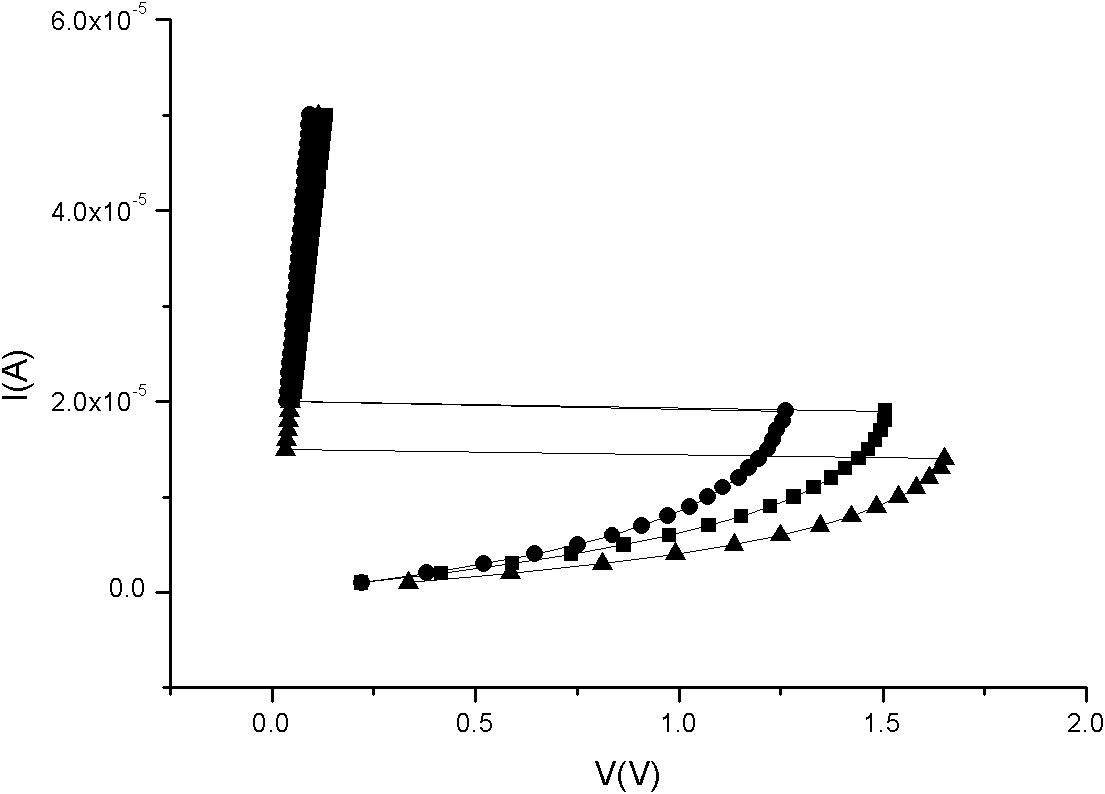
[0038] In this embodiment, the phase change material thin film is deposited on the substrate with Al lower electrode and W heating electrode. The specific conditions of sputtering are: use Sb 2 Te 3 target and SiO 2 In the method of target co-sputtering, Ar gas with a purity of 99.999% is introduced simultaneously during the co-sputtering process, and the gas flow rate of Ar is 20 sccm. Sb 2 Te 3 target and SiO 2 Targets use RF power, Sb 2 Te 3 The power of the target is set to 20W, SiO 2 The power is set to 15W, the sputtering time is 30min, and the film thickness is about 120nm.
[0039] see image...
PUM
| Property | Measurement | Unit |
|---|---|---|
| thickness | aaaaa | aaaaa |
Abstract
Description
Claims
Application Information


