Thin film transistor on basis of metal oxide and preparation method and application thereof

A thin-film transistor and oxide thin-film technology, applied in transistors, semiconductor/solid-state device manufacturing, electrical components, etc., can solve the problems of difficult to use display backplanes, difficult to large-scale, slow film deposition rate, etc. area and the effect of mass production and low cost

Inactive Publication Date: 2012-06-27
GUANG ZHOU NEW VISION OPTO ELECTRONICS TECH
View PDF5 Cites 21 Cited by
  • Summary
  • Abstract
  • Description
  • Claims
  • Application Information

AI Technical Summary

Problems solved by technology

However, due to the growth method of ALD monoatomic layer deposition, the film deposition rate is too slow,

Method used


Image

  • Thin film transistor on basis of metal oxide and preparation method and application thereof
  • Thin film transistor on basis of metal oxide and preparation method and application thereof
  • Thin film transistor on basis of metal oxide and preparation method and application thereof

Examples


Example Embodiment

[0047] Example 1

[0048] Method of fabricating thin film transistors using back channel etch structure (BCE):

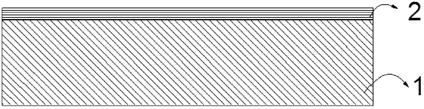
[0049] (1) If figure 1 As shown, 200 nm thick SiO was deposited using PECVD on a 0.5 mm thick alkali-free glass substrate 1 2 layer as buffer layer 2;

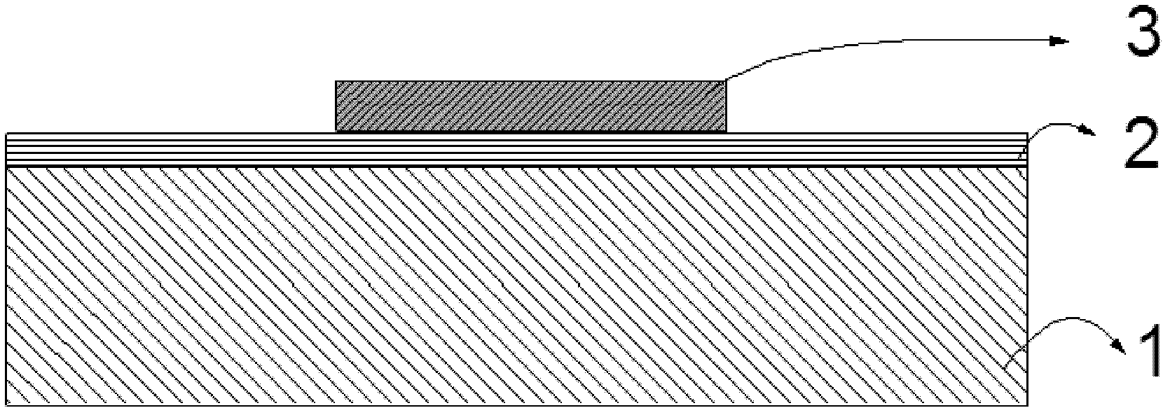
[0050] (2) If figure 2 As shown, on the buffer layer, an Al-Ce (Al:Ce=3at%) alloy target is used to deposit a 300nm Al-Ce alloy film as gate metal 3 by magnetron sputtering, and photolithography is used process to pattern it to form a gate metal layer;

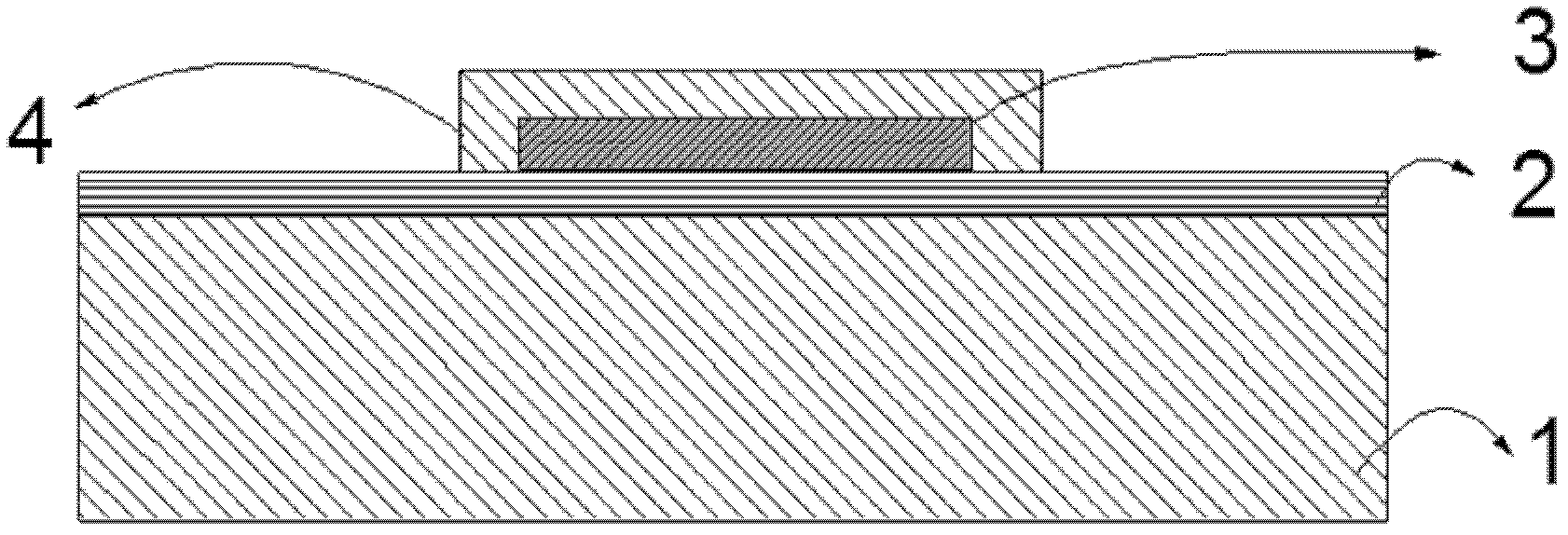
[0051] (3) Spin-coating photoresist on the patterned Al-Ce film, and then patterning the photoresist through exposure and development. Using the photoresist as a mask, the part of the Al-Ce film covered with the photoresist will not be oxidized to Al 2 O 3 -CeO 2 .

[0052] (4) Use electrolyte: ethylene glycol+ammonium salicylate+deionized water, the weight ratio is 49:1:50. The oxidation voltage was set to 100V, and the gate insulating layer 4 was formed...

Example Embodiment

[0058] Example 2

[0059] Method of fabricating thin film transistors using etch stop layer structure (ESL):

[0060] (1) If Figure 8 As shown, 50 nm thick SiN was deposited using PECVD on a 0.5 mm thick alkali-free glass substrate 1 x layer as the buffer layer 2.

[0061] (2) If Figure 9 As shown, a 200 nm Al-Hf (Al:Hf=10 at%) thin film was deposited on the buffer layer 2 as a gate metal. The gate metal layer 3 is formed by patterning the Al-Hf thin film using a photolithography process.

[0062] (3) Spin-coating photoresist on the patterned Al-Hf film, and then patterning the photoresist through exposure and development. Using the photoresist as a mask, the part covering the photoresist on the Al-Hf film will not be oxidized (by exposure and development, the photoresist remains only on the Al film that needs to be protected).

[0063] (4) If Figure 10 As shown, the anodic oxidation method is used, and the electrolyte is a mixed solution of ethylene glycol + ammonia...


PUM

PropertyMeasurementUnit
Thicknessaaaaaaaaaa
Thicknessaaaaaaaaaa
Thicknessaaaaaaaaaa

Abstract

The invention discloses a thin film transistor on the basis of metal oxide and a preparation method and application thereof. The preparation method comprises the following steps of: (1) making a buffer layer; (2) depositing a gate metal layer on the buffer layer; (3) preparing a gate insulation layer on the gate metal layer by using an anodic oxidation method, wherein the part in the gate metal layer, on which an oxide film does not need to be deposited, is protected by using a photoresist; (4) removing the photoresist; (5) removing an unrequired metal lead; (6) preparing an active layer on the gate insulation layer; and (7) according to the designed thin film transistor structure, depositing and patterning source and drain electrodes, a pixel electrode and a protection layer or an etched barrier layer. According to the invention, pure Al or Al alloy is used as gate metal and the gate insulation layer is prepared by using the anodic oxidation method. The performance of the gate insulation layer can be changed by regulating the components of the gate metal, so that the electrical properties of the thin film transistor are improved.

Description

technical field [0001] The invention relates to a preparation method of a thin film transistor. In particular, it relates to a preparation method of a gate insulating layer of a metal oxide semiconductor thin film transistor. Background technique [0002] Thin film transistors (TFTs) are currently mainly used to drive sub-pixels of liquid crystal displays (LCD) and organic light emitting diode (OLED) displays. The drive backplane made of thin film transistor arrays is a key component for the display screen to achieve higher pixel density, aperture ratio and improved brightness. At present, TFT-LCD generally adopts a TFT backplane based on amorphous silicon as the active layer. However, due to the low mobility of amorphous silicon (0.1cm 2 V -1 s -1 left and right), can not meet the requirements of OLED display, high-definition TFT-LCD and 3D display. As the active layer material of thin film transistor, metal oxide semiconductor is regarded as the next generation of d...

Claims


Application Information

Patent Timeline
IPC IPC(8): H01L29/786H01L21/441H01L21/445
Inventor 徐苗罗东向邹建华陶洪兰林锋王磊彭俊彪
Owner GUANG ZHOU NEW VISION OPTO ELECTRONICS TECH
Why Eureka
Try Eureka