GaN-based high-electron-mobility transistor and manufacturing method thereof

A high electron mobility, gallium nitride-based technology, applied in the field of gallium nitride-based high electron mobility transistors and their fabrication, can solve problems such as insufficiently meeting the requirements of high electron mobility transistors

Inactive Publication Date: 2012-07-04
山东淮数大数据产业发展有限公司
View PDF4 Cites 10 Cited by
  • Summary
  • Abstract
  • Description
  • Claims
  • Application Information

AI Technical Summary

Problems solved by technology

But this device is still not enough to meet the high electron mobility transistor requirements

Method used


Image

  • GaN-based high-electron-mobility transistor and manufacturing method thereof
  • GaN-based high-electron-mobility transistor and manufacturing method thereof
  • GaN-based high-electron-mobility transistor and manufacturing method thereof

Examples


Embodiment 1

[0034] Embodiment 1: sapphire substrate

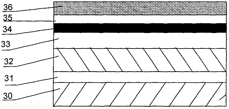
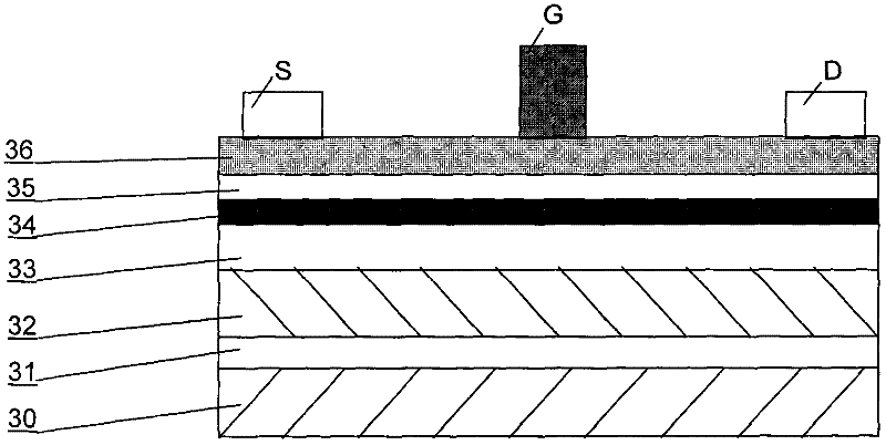
[0035] First, the sapphire substrate is cleaned at high temperature for 10 minutes. Then grow an aluminum nitrogen buffer layer 31 on the sapphire (0001) surface at a growth temperature of 1100° C. and a growth thickness of 30 nm.

[0036] A layer of high-resistance gallium nitride layer 32 is grown on the aluminum nitrogen buffer layer 31 with a thickness of 3 μm and a growth temperature of 1120° C.

[0037] A gallium nitride channel layer 33 is grown on the high-resistance gallium nitride layer 32 with a thickness of 30 nm and a growth temperature of 1080° C.

[0038] An indium nitrogen insertion layer 34 is grown on the gallium nitride channel layer 33 with a thickness of 10 nm and a growth temperature of 650° C. This layer contains indium nitrogen, which has the smallest electron effective mass among all group III nitride semiconductors, has high mobility and high saturation velocity. Thereby improving the mobility of the device...

Embodiment 2

[0041] Example 2: Silicon carbide substrate

[0042] First, the silicon carbide substrate is cleaned at high temperature for 10 minutes; the aluminum nitrogen buffer layer 31 is grown again at a growth temperature of 1100° C. and a growth thickness of 30 nm.

[0043] A layer of high-resistance gallium nitride layer 32 is grown on the aluminum nitrogen buffer layer 31 with a thickness of 3 μm and a growth temperature of 1120° C.

[0044] A gallium nitride channel layer 33 is grown on the high-resistance gallium nitride layer 32 with a thickness of 30 nm and a growth temperature of 1080° C.

[0045] An indium nitrogen insertion layer 34 is grown on the gallium nitride channel layer 33 with a thickness of 10 nm and a growth temperature of 650° C.

[0046] An AlN insertion layer 35 is grown on the InN insertion layer 34 with a thickness of 8nm and a growth temperature of 1100°C.

[0047] An AlGaN barrier layer 36 is grown on the AlN insertion layer 35 with a thickness of 30nm, t...


PUM

PropertyMeasurementUnit
thicknessaaaaaaaaaa
thicknessaaaaaaaaaa
thicknessaaaaaaaaaa

Abstract

The invention relates to a GaN-based high-electron-mobility transistor and a manufacturing method thereof, wherein a transistor structure comprises an aluminum nitrogen buffer layer grown on a substrate, a high-resistance GaN layer grown on the aluminium nitrogen buffer layer, and a high-mobility GaN channel layer grown on the high-resistance GaN layer. The transistor is characterized in that an indium nitrogen insert layer is grown on the high-mobility GaN channel layer, and an aluminum nitrogen insert layer is grown on the indium nitrogen insert layer; and an unintentional adulteration aluminium gallium nitrogen layer is grown on the aluminium nitrogen insert layer, and the aluminium nitrogen insert layer and the unintentional adulteration aluminium gallium nitrogen layer form a barrier layer together. According to the invention, the indium nitrogen insert layer is utilized to effectively reduce alloy scattering, increase the electron mobility and electron concentration of the high electron mobility transistor and improve the stability and reliability of a transistor device.

Description

technical field [0001] The invention belongs to the technical field of semiconductors, and in particular relates to a gallium nitride-based high electron mobility transistor and a manufacturing method thereof. Background technique [0002] Gallium nitride (GaN) has excellent physical, chemical and mechanical properties. GaN has good chemical stability, insoluble in water, acid and alkali at room temperature, has high breakdown electric field, high electron saturation velocity and peak velocity, large forbidden band width (3.4eV), and good radiation resistance . As a result, it has great application prospects in the fields of optoelectronics and microelectronics, and has become a typical representative of the third-generation semiconductor materials. GaN-based AlGaN / GaN high electron mobility transistors have become one of the most important devices in the field of microelectronics, and play an important role in communication and radar, aerospace, automotive electronics and...

Claims


Application Information

Patent Timeline
Patent Type & Authority Applications(China)
IPC IPC(8): H01L29/778H01L29/205H01L21/335
Inventor 张洪月曲爽李树强王成新徐现刚
Owner 山东淮数大数据产业发展有限公司
Why Eureka
Try Eureka