Eureka AIR delivers breakthrough ideas for toughest innovation challenges, trusted by R&D personnel around the world.

Preparation method of insulator silicon dioxide film in MIM (metal-insulator-metal) type capacitor

A technology of silicon dioxide and insulators, which is applied in semiconductor/solid-state device manufacturing, circuits, electrical components, etc., can solve the problems of poor film properties, poor barrier film quality, low thermal oxygen reaction, etc., achieve good electrical stability, improve performance effect

Inactive Publication Date: 2012-07-25
SHANGHAI HUALI MICROELECTRONICS CORP
View PDF6 Cites 0 Cited by
  • Summary
  • Abstract
  • Description
  • Claims
  • Application Information

AI Technical Summary

Problems solved by technology

[0006] image 3 Prepare the infrared spectrogram of silicon dioxide thin film for SACVD method in the background technology of the present invention; image 3 As shown, since the properties of the silicon oxide film of the insulating layer directly determine the performance of the MIM capacitor, the requirements for the properties of the film are relatively high, but the temperature of SACVD is relatively low in the deposition process compared to the thermal oxygen reaction of the furnace tube, and there is no plasma The bombardment effect of the body, the film will contain a large number of Si-OH bonds, and the film contains a certain amount of H, which will cause the properties of the film to be relatively poor. In the actual production process, due to the barrier of the self-aligned silicide region The quality of the film is poor, and it cannot well block the boron precipitation in the source and drain regions and cause defects

Method used


Image

  • Preparation method of insulator silicon dioxide film in MIM (metal-insulator-metal) type capacitor
  • Preparation method of insulator silicon dioxide film in MIM (metal-insulator-metal) type capacitor
  • Preparation method of insulator silicon dioxide film in MIM (metal-insulator-metal) type capacitor

Examples


Embodiment Construction

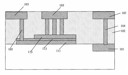
[0026] The specific embodiment of the present invention will be further described below in conjunction with accompanying drawing:

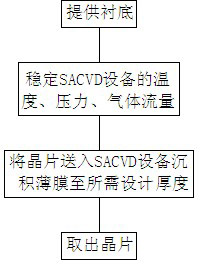
[0027] Figure 4 It is the process flow chart of the preparation method of silicon dioxide film of insulator in the MIM type electric capacity of the present invention;

[0028] Figure 5-9 It is a schematic structural flow diagram of a method for preparing an insulator silicon dioxide film in a MIM type capacitor of the present invention.

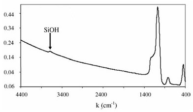
[0029] Such as Figure 4-9 As shown, a wafer is provided as a substrate 1, after stabilizing the gas flow, pressure and temperature of the SACVD equipment, the substrate 1 is placed in the SACVD equipment, and the first layer of silicon dioxide film 2 is deposited on the substrate 1, Afterwards, a passivation dehydrogenation treatment process 11 is carried out for 5-50 minutes using a mixed gas containing active oxygen atoms or ozone gas to remove H in Si-H in the first layer of silicon dioxide film 2; then...


PUM


Abstract

The invention relates to the field of semiconductor manufacturing, particularly to a preparation method of an insulator silicon dioxide film in a MIM (metal-insulator-metal) type capacitor. According to the preparation method of the insulator silicon dioxide film in the MIM type capacitor, provided by the invention, an entire deposition process of the silicon dioxide film can be finished through cyclic processes of multiple sub atmosphere chemical vapor depositions and the passivating dehydrogenating treatment technology, and therefore, the Si-OH bond existed in the film is effectively removed, and the performance of the silicon dioxide film in MIM is improved; and the insulator silicon dioxide film in the MIM type capacitor is good in electrical stability.

Description

technical field [0001] The invention relates to the manufacturing field of semiconductor integrated circuits, in particular to a method for preparing an insulator silicon dioxide film in a MIM capacitor. Background technique [0002] Sub Atmospheric Chemical Vapor Deposition (Sub Atmosphere Chemical Vapor Deposition, referred to as SACVD) is a widely used chemical vapor deposition technology. The thermochemical reaction is carried out between 300-500°C. Since the reaction pressure is generally 50-600torr, which is slightly lower than atmospheric pressure, it is called sub-atmospheric chemical vapor deposition. [0003] Since SACVD does not need to use plasma to dissociate the reaction gas during the reaction process, but generates silicon dioxide through the reaction of active oxygen atoms in ozone and silicon in TEOS, therefore, the silicon dioxide film (insulating layer) prepared by SACVD method ) has no plasma-induced damage (Plasma Induced Damage, PID) to the substrate ...

Claims


Application Information

Patent Timeline
IPC IPC(8): C23C16/44C23C16/40H01L21/02
Inventor 徐强毛智彪
Owner SHANGHAI HUALI MICROELECTRONICS CORP
Why Eureka
Eureka Blog
Learn More