Method for low-temperature solid bonding of semiconductor device
A semiconductor and bonding technology, applied in the fields of semiconductor devices, semiconductor/solid-state device manufacturing, electric solid-state devices, etc., can solve the problems of thermal damage to the device, difficult to completely remove the solder, etc., to avoid thermal damage, controllable interface reaction, simplification The effect of the process flow
- Summary
- Abstract
- Description
- Claims
- Application Information
AI Technical Summary
Problems solved by technology
Method used
Image

Examples
Embodiment 1
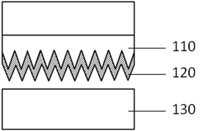
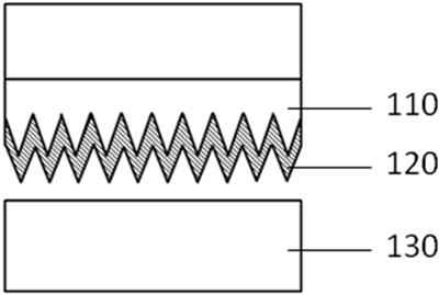
[0039] Formation of bumped under metal layer (UBM), copper pillar bumps, Ni barriers and bumps on bare die with I / O pads by standard photolithographic patterning, sputter deposition and electrochemical deposition For the Sn layer on the surface, the typical copper pillar bump size is 60 μm in diameter and 40 μm in height. A typical Ni barrier layer thickness is about 1 μm. A typical Sn layer thickness is 3 - 5 μm, with a height difference of less than 0.5 μm. Copper microneedle cones and surface oxidation-resistant Au layer are prepared by chemical deposition or electrochemical deposition on the pad area of the flip-chip substrate. The height of the needle cones can be 1 μm-5 μm. In this example, the height of the needle cones is about 5 μm. The thickness of Au can be 5nm-50nm, in this example, the thickness of Au is about 10nm. This thickness of Au coating will not affect the needle cone morphology. Fix the chip and the substrate face-to-face on the flip-chip b...
Embodiment 2
[0041] The lower metal layer (UBM) and Sn layer with I / O pads on the front side and the I / O pads on the front side of the bare chip through the through-silicon via (TSV) to the device side are bumped, typically The thickness of the Sn layer is 2 - 5 μm, and the height difference is less than 0.5 μm. The chip is usually thinned to less than 100 μm, and the copper microneedle cone group and the anti-oxidation gold layer are prepared on the surface of the ground and exposed TSV filling metal. The height of the needle cone is about 3 - 5 μm, and the thickness of Au is about 10 nm. After using plasma to remove the surface oxide layer and contamination particles, two or more silicon wafers with this structure are stacked and fixed in the bonding machine, and the temperature is raised to a bonding temperature of 190 ° C. At the same time, the bonding machine applies 10 The equivalent static pressure of MPa is maintained for 3 minutes to complete the stacking bonding.
Embodiment 3
[0043]Prepare a copper microneedle cone layer and an anti-oxidation Au layer on the metal block of the pad area of the printed circuit board (PCB) for ball grid array (BGA) surface mounting. The needle cone height is about 3 - 5μm, and the gold thickness is about 10nm. The BGA package planted with Sn alloy solder balls with a size of 300 - 800 μm is pickled to remove the oxide layer on the surface of the solder balls, and fixed and aligned with the PCB in the bonding machine, and the temperature is raised to a bonding temperature of 190 ° C. At the same time, an equivalent static pressure of 10 MPa is applied by the bonding machine and kept for 3 minutes to complete the stack bonding.
PUM
 Abstract
Description
Claims
Application Information