

Electrochemical etching of semiconductors
A semiconductor and current technology, applied in semiconductor devices, semiconductor/solid-state device manufacturing, circuits, etc., can solve the problems of damaged diode performance loss, increased process time and cost, and complicated preparation process, so as to eliminate complicated steps and improve reliability. sexual effect
- Summary
- Abstract
- Description
- Claims
- Application Information
AI Technical Summary
Problems solved by technology
Method used
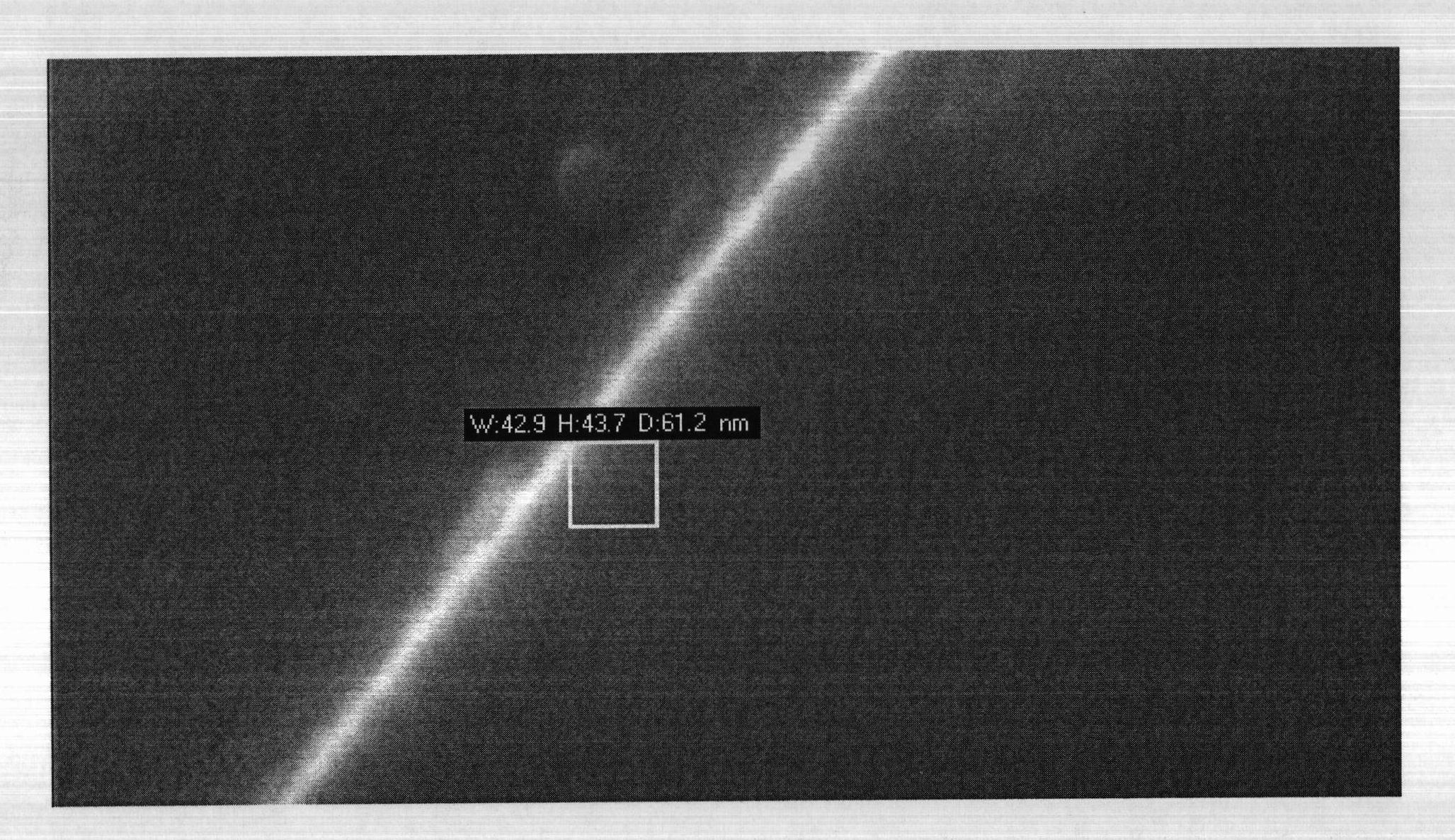
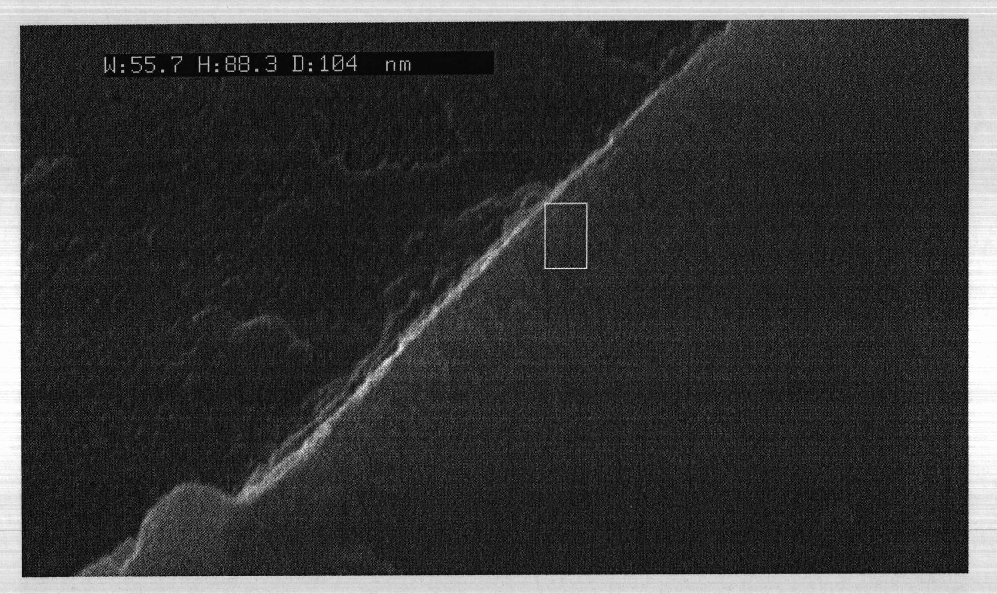
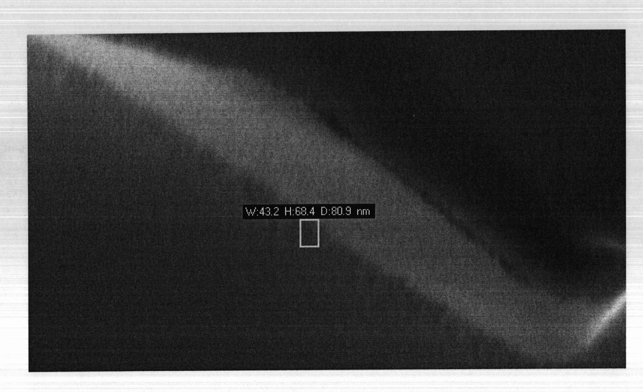
Image

Examples
Embodiment 1
[0056] A doped monocrystalline silicon wafer having pyramidal bumps on its front side is provided. The wafer has n+ doped regions on the front side of the wafer forming the emissive layer. The wafer also has a PN junction below the emissive layer. The front side of the wafer is coated with SiN x Composed of anti-reflection layer. The front side of the wafer has a pattern for current paths that passes through the anti-reflection layer, exposing the surface of the silicon wafer. Each current path spans the entire length of the wafer. The current paths are bonded to busbars at one end of the wafer and at the center of the wafer. The backside of the wafer is p+ doped and contains aluminum electrodes.
[0057] The wafer was immersed in a 1 wt% hydrofluoric acid solution to clean the current paths and busbars. Wash for one minute at room temperature. The wafer was rinsed with water. In addition to removing contaminants from the wafer, the hydrofluoric acid solution also remo...
Embodiment 2
[0062] The method described above in Example 1 was repeated except that silver was electroplated on the nickel seed layer instead of copper. Use ENLIGHT TM Silver Plate 620 silver electroplating bath plated silver. The current density is 1.5A / dm 2And the plating is finished for 10 minutes. Artificial light was also applied to the wafer throughout the plating. The light source is a 250 watt halogen lamp. Plating temperatures range from 20°C to 40°C. An 8-10 μm layer of silver is deposited on this nickel.
[0063] The adhesion of the metal layer was tested using the ASTM D3359-97 standard tape test. Adhesion at the interface between the nickel and the silicon wafer was unacceptable in all current paths and busbars.
Embodiment 3
[0065] A single crystal wafer of the same type as in the previous Example 1 was provided. The wafer was placed on a metal plating support with the backside aluminum electrode in direct contact with the metal plating support. The interface between the cell and the support was sealed around the circumference of the wafer to minimize solution penetration between the back of the cell and the plating support. During the anode cycle, current from the rectifier flows through the holder and into the cell through the back contact.
[0066] Afterwards, the current paths and busbars were oxidized using 5 wt% hydrogen peroxide aqueous solution to ensure that the silicon surface was oxidized. Thereafter, the wafers mounted on supports described in the previous paragraphs were immersed in an aqueous composition in the electroplating tank comprising 10 g / L of nickel ions from nickel sulfamate, 45 g / L of sodium bifluoride, and 15 g / L of L sulfamic acid. The holder with the wafer was connec...
PUM
| Property | Measurement | Unit |
|---|---|---|
| depth | aaaaa | aaaaa |
| depth | aaaaa | aaaaa |
| depth | aaaaa | aaaaa |
Abstract
Description
Claims
Application Information