Method for preparing high-power microwave chip type multilayer ceramic dielectric capacitor

A technology of capacitors and microwave chips, which is applied in the direction of laminated capacitors, fixed capacitor electrodes, and parts of fixed capacitors. Layer ceramic capacitors can not wait for the problem

Active Publication Date: 2012-09-19
蒋永昭
View PDF5 Cites 5 Cited by
  • Summary
  • Abstract
  • Description
  • Claims
  • Application Information

AI Technical Summary

Problems solved by technology

[0007] The purpose of the present invention is to solve the problem that the chip multilayer ceramic capacitors prepared by the existing casting method cannot be used as high-power capacitors for high-voltage pulse circuits and the chip multilayer ceramic capacitors prepared with general ceramic materials cannot be used as microwave power capacitors. for microwave circuits
The reason is that the existing chip multilayer ceramic capacitors will be burned in high-voltage pulse high-current and microwave high-power circuits
[0008] On the basis of exploring the theory of dielectric and electric conduction of multilayer ceramic capacitors, the present invention solves the problem of electrode current caused by the defect by eliminating the defect of the mixed layer of the internal electrode and the medium in the multilayer structure of the existing multilayer ceramic capacitor. Loss and high-frequency insertion loss increase to cause the capacitor to burn out; at the same time, a low-fired ceramic material with a sintering temperature lower than 980°C has been developed to make the inner electrode of the multilayer ceramic capacitor have higher conductivity and lower electrode current loss

Method used


Image

  • Method for preparing high-power microwave chip type multilayer ceramic dielectric capacitor
  • Method for preparing high-power microwave chip type multilayer ceramic dielectric capacitor
  • Method for preparing high-power microwave chip type multilayer ceramic dielectric capacitor

Examples


Embodiment 1

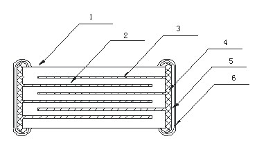
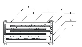
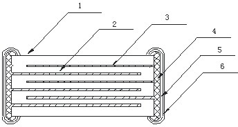
[0042] Such as figure 1 As shown, it consists of multi-layer porcelain dielectric layer, internal electrode layer and three-layer terminal electrode.

[0043] The palladium-silver paste electrode layers on both sides of the ceramic medium are printed in the same pattern, so only one side has a palladium-silver layer at both ends, and each palladium-silver inner electrode layer is electrically connected to the terminal electrode at the end (in this manual) Electrical connection means that there is an electrical connection between two parts, which can be a contact connection, a wire connection, or a conductive connection through other parts).

[0044] From figure 1 It can be seen that the stacked chip multilayer ceramic capacitor has six surfaces, where the surfaces at both ends expose the palladium-silver layer, and a silver electrode layer 4 is provided, and a nickel layer 5 and a tin layer 6 are electroplated on the silver electrode layer 4. , The silver electrode layer 4...

Embodiment 2

[0046] Preparation of a microwave multilayer ceramic capacitor with a working voltage of 500V and a capacitance of 150pF

[0047] a. Put the material-bearing aluminum plate on the base of the medium paste printing machine, and print a layer of 85×85mm on the material-bearing aluminum plate through the non-mark printing method (the size of the hollow non-polyester film is 85×85mm) , a niobium-bismuth-zinc porcelain dielectric slurry film with a thickness of 100 μm, remove the aluminum plate as the material, and dry it in a tunnel oven at 120 ° C for 7 minutes; b. Lower the base of the aluminum plate for the material by 100 μm, repeat the above process After 3 times, an attached piece of the capacitor was formed on the receiving aluminum plate; c. Put the receiving aluminum plate on the base of another printing machine for printing electrodes, and print the product on the surface of the attached sheet. For the electrode paste pattern of 506 capacitors, remove the aluminum plate,...

Embodiment 3

[0050] Preparation of high-power multilayer ceramic capacitors with a working voltage of 1500V and a capacitance of 0.15μF

[0051] a. Put the material-bearing aluminum plate on the base of the medium paste printing machine, and print a layer of 80×80mm on the material-bearing aluminum plate through the non-mark printing method (the size of the hollow non-polyester film is 80×80mm) , a barium titanate porcelain dielectric slurry film with a thickness of 100 μm, remove the aluminum plate as the material, and dry it in a tunnel oven at 130 ° C for 8 minutes; b. Lower the base of the aluminum plate for the material by 100 μm, and repeat the above process After 3 times, an attached sheet of the capacitor was formed on the receiving aluminum plate; c. Put the receiving aluminum plate on the base of another printing machine for printing electrodes, and print 24 electrode paste patterns of capacitors on the surface of the attached sheet, Remove the material-bearing aluminum plate, an...


PUM

PropertyMeasurementUnit
thicknessaaaaaaaaaa
thicknessaaaaaaaaaa
thicknessaaaaaaaaaa

Abstract

The invention discloses a method for preparing a high-power microwave chip type multilayer ceramic dielectric capacitor. The method comprises the following steps of: carrying out printing for multiple times with a traceless printing method to form an attached chip of the capacitor; printing a designed inner electrode paste figure on the attached chip, and forming an inner electrode membrane layer of multiple capacitors after carrying out drying; carrying out drying after printing a layer of ceramic dielectric paste membrane on a ceramic dielectric layer with an inner electrode layer by use of the traceless printing method; placing a designed staggering bar in the inner electrode extraction direction of the capacitors; carrying out drying after printing another inner electrode membrane layer of the capacitors by the process; repeating the processes to form another attached chip of the capacitor; and carrying out row adhesion, cutting, sintering, end barreling, terminal electrode preparation, and terminal electronickelling, electrotinning and the like. The method aims at solving the problems that power loss and high-frequency insertion loss caused by the inner electrode loss of the existing chip type multilayer ceramic dielectric capacitor are great, and the capacitor is liable to being broken down and burnt by currents in a high voltage pulse and a microwave high-power circuit.

Description

technical field [0001] The invention relates to a preparation method of a fixed capacitor for electronic equipment, in particular to a preparation method of a high-power, microwave chip multilayer ceramic capacitor. Background technique [0002] New-type chip electronic components are the National Science and Technology Ministry's "10th and 25th Five-Year Plan" new technology research and development planning projects, and high-power, microwave chip multilayer ceramic capacitors are still a blank in China. [0003] High-power, microwave chip multilayer ceramic capacitors are one of the important electronic components used in microwave frequency band electronic equipment. With the advancement of modern communication technology, satellite broadcasting technology and military electronic equipment, a new type of electronic capacitor has been developed rapidly. Components play a vital role in the progress of miniaturization, integration and high reliability of electronic equipme...

Claims


Application Information

Patent Timeline
Patent Type & Authority Applications(China)
IPC IPC(8): H01G4/30H01G4/005H01G4/12
CPCY02E60/13
Inventor 蒋永昭蒋楠薛爱伦
Owner 蒋永昭
Why Eureka
Try Eureka