Up-and-down-conversion luminescent high-transmittance amorphous fluoride film and preparation method thereof

A fluoride and thin film technology, applied in the field of high-transparency amorphous fluoride thin film and its preparation, can solve problems such as low transmittance, achieve the effects of high transmittance, improve photoelectric conversion efficiency, and reduce light reflection

Active Publication Date: 2012-10-10
BEIJING UNIV OF TECH
View PDF4 Cites 7 Cited by
  • Summary
  • Abstract
  • Description
  • Claims
  • Application Information

AI Technical Summary

Problems solved by technology

Comparing the above materials, it is found that the transmittance is low. Among them, the fluoride light-converting film prepared by

Method used


Image

  • Up-and-down-conversion luminescent high-transmittance amorphous fluoride film and preparation method thereof
  • Up-and-down-conversion luminescent high-transmittance amorphous fluoride film and preparation method thereof
  • Up-and-down-conversion luminescent high-transmittance amorphous fluoride film and preparation method thereof

Examples


Embodiment 1

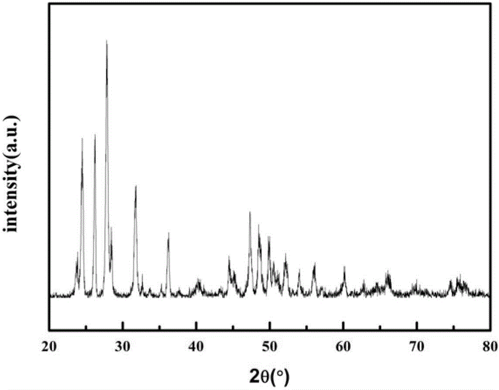
[0032] (1) In YbF 3 Add ErF to the powder 3 Powder, where ErF 3 The mole fraction of the powder is 5%, then ball milled and mixed, dried and pressed into tablets, and calcined at 600°C for 8 hours by carbon coating to make a ceramic target. The XRD pattern of its ceramic target material (see figure 1 ) basically conforms to YbF 3 PDF 34-0102 Diffraction Standard Spectrum.

[0033] (2) YbF prepared by the above method 3 : Er ceramic target material, using electron beam deposition method: using silicon wafer as the substrate, under vacuum conditions, the substrate temperature is 500°C, the target distance is 32cm, the deposition beam current is 4, and the deposition time is 15min to obtain YbF 3 film.

Embodiment 2

[0035] (1) In YbF 3 Add ErF to the powder 3 Powder, where ErF 3 The mole fraction of the powder is 5%, and then ball milled and mixed, dried and pressed into tablets, and calcined at 650°C for 8 hours by carbon coating, and fired into a ceramic target.

[0036] (2) YbF prepared by the above method 3 : Er ceramic target material, using electron beam deposition method: using silicon wafer as the substrate, under vacuum conditions, the substrate temperature is 500 ℃, the target distance is 32cm, the deposition beam current is 3, and the deposition time is 60min to obtain YbF 3 film, its XRD pattern is shown in figure 2 .

Embodiment 3

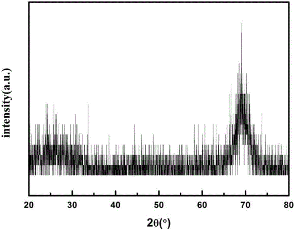
[0038] (1) In YbF 3 Add ErF to the powder 3 Powder, where ErF 3 The mole fraction of the powder is 10%, then ball milled and mixed, dried and pressed into tablets, and calcined at 750°C for 8 hours by carbon coating to make a ceramic target. Its XRD pattern is shown in image 3 .

[0039] (2) YbF prepared by the above method 3 : Er ceramic target material, using the electron beam deposition method: using a silicon wafer as the substrate, under vacuum conditions, the substrate temperature is 500°C, the target distance is 32cm, the deposition beam current is 5, and the deposition time is 60min to obtain YbF 3 film, its XRD pattern is shown in Figure 4 . Use the FLS920 fluorescence spectrometer to measure the emission spectrum at room temperature under the excitation condition of 378nm. For the emission spectrum, see Figure 5 ; For the luminescence spectrum excited at 980nm see Figure 6 .


PUM


Abstract

The invention discloses an up-and-down-conversion luminescent high-transmittance amorphous fluoride film and a preparation method thereof, and belongs to the field of solid luminescent materials. The film comprises YbF3 and ErF3, and the molar fraction of the ErF3 is 0.5%-15%. The preparation method includes: adding YbF3 powder into ErF3 powder for ball-milling mixing, drying prior to tabletting, and calcining for 6h-8h at the temperature of 600-750 DEG C by a carbon coating method so that a ceramic target is calcined; and using an electron beam deposition method which includes that a silicon wafer and quartz are used as a substrate, and under the vacuum condition, the substrate temperature ranges from 400 DEG C to 500 DEG C, the target spacing ranges from 25cm to 32cm, the deposition beam current ranges from 3mA to 6mA, and the deposition time ranges from 15min to 90min. The amorphous film achieves combination of up-conversion and down-conversion mechanisms and is capable of effectively converting an ultraviolet wave band (300nm-400nm) and an infrared wave band (around 980nm) to a visible light wave band (around 656nm), and the transmittance of the film is averagely higher than 95% so that the film is hopefully applied to solar cells to improve photoelectric efficiency of the same.

Description

technical field [0001] The invention belongs to the field of rare earth luminescent materials, and in particular relates to a highly transparent amorphous fluoride thin film with up-down light conversion and a preparation method thereof. Background technique [0002] The study of solar cell materials has attracted great attention and attention due to the increasingly urgent energy issues. However, due to the constraints of semiconductor band gaps, various solar cells can only achieve high-efficiency photoelectric conversion for light in their specific spectral ranges. , For example, for amorphous silicon (Eg=1.75eV) solar cells, the best spectral response range is 500nm~600nm, when the light wavelength extends to the long-wave direction and short-wave direction respectively, the response intensity to light decreases rapidly. [0003] For this reason, many people are looking for ways to expand the spectral response range of the battery to increase its conversion efficiency, b...

Claims


Application Information

Patent Timeline
IPC IPC(8): C09K11/85C23C14/06C23C14/30H01L31/055
CPCY02E10/50Y02E10/52
Inventor 王如志张影曲铭浩严辉张铭王波宋雪梅朱满康侯育冬刘晶冰汪浩
Owner BEIJING UNIV OF TECH
Why Eureka
Try Eureka