Integrated preparation method for LED fluorescent powder coating

A phosphor and coating technology, applied in electrical components, circuits, semiconductor devices, etc., can solve problems such as electrode pattern separation, and achieve the effect of improving optics and overall performance

Inactive Publication Date: 2012-10-10
UNIV OF ELECTRONIC SCI & TECH OF CHINA
View PDF5 Cites 12 Cited by
  • Summary
  • Abstract
  • Description
  • Claims
  • Application Information

AI Technical Summary

Problems solved by technology

[0006] The problem to be solved by the present invention is how to use the powder-slurry process based on the photosensitive principle to realize the integrated coating of the phosphor powder coating (conformal coating) of the LED chip, and to provide a phosphor coating slurry for wafer-level packaging

Method used


Image

  • Integrated preparation method for LED fluorescent powder coating
  • Integrated preparation method for LED fluorescent powder coating
  • Integrated preparation method for LED fluorescent powder coating

Examples


Embodiment 1

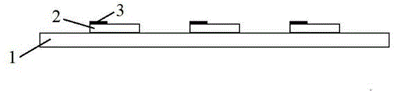
[0072] Take polyvinyl alcohol (PVA), photosensitive agent ammonium dichromate (ADC), phosphor powder and deionized water and mix evenly to form a stable powder PVA dispersion containing phosphor particles. The phosphor powder photosensitive adhesive dispersion is coated on the surface of the LED chip (Wafer, wafer) by the overmolding method, and the required coating thickness is controlled.

[0073] Air-dried or oven-dried, exposed with an external light source (blue light or ultraviolet light) combined with a mask plate, developed with hot water, and obtained a phosphor powder photosensitive adhesive dispersion coating pattern on the surface of the LED chip in the light-emitting direction.

[0074] Put the LED chip with the coating pattern of phosphor photosensitive adhesive dispersion into the plasma degumming equipment, and use the method of oxygen plasma bombardment to remove the organic components in the coating to obtain a powder layer containing phosphor particles.

[0...

Embodiment 2

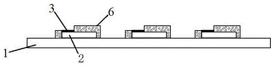
[0078]Mix polyvinyl alcohol (PVA), diazo resin, phosphor powder and deionized water in a certain proportion (2%: 0.02%: 17.98%: 80%) to form a stable dispersion of diazo photosensitive adhesive containing phosphor particles body.

[0079] Spinning is used to coat the phosphor powder photosensitive adhesive dispersion on the surface of the LED chip (wafer) to control the coating requirements of a certain thickness.

[0080] Air-dried or oven-dried, exposed with an ultraviolet or blue light source combined with a mask plate, and then developed with hot water to obtain a phosphor powder photosensitive adhesive dispersion coating pattern on the surface of the LED chip in the light-emitting direction.

[0081] Put the LED chip (Wafer) with the photosensitive adhesive pattern of the phosphor into the plasma degumming equipment, and use the method of argon / hydrogen (85 / 15) plasma bombardment to remove the organic components in the photosensitive adhesive, and obtain the phosphor with...

Embodiment 3

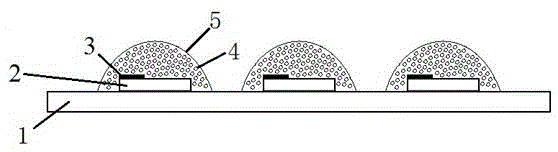
[0085] Take polyvinyl alcohol (PVA), diazo resin, fluorescent powder, nano-titanium dioxide powder and deionized water and mix evenly to form a stable PVA photosensitive adhesive dispersion containing fluorescent powder particles.

[0086] Use the dipping method (Flowing) to coat the phosphor powder photosensitive adhesive dispersion on the surface of the LED chip (wafer wafer) to control the required thickness.

[0087] Dry it with hot air, expose it with an ultraviolet light source combined with a mask plate, develop it with hot water, and get a phosphor powder photosensitive adhesive dispersion coating pattern on the surface of the LED chip (Wafer) in the light emitting direction.

[0088] Put the LED chip (Wafer) coated with phosphor photosensitive adhesive into a baking oven, bake at 300~500°C for a period of time, heat and oxidize, remove the organic components in the photosensitive adhesive, and obtain the determination of the phosphor powder layer pattern.

[0089] Sp...


PUM


Abstract

The invention discloses an integrated preparation method for an LED fluorescent powder coating, which belongs to the photoelectric technical field. The method comprises the following steps: (1), preparing fluorescent powder and sensitive colloid dispersion; (2), spinning the fluorescent powder to form a fluorescent powder-sensitive colloid dispersion coating; (3), obtaining fluorescent powder-sensitive colloid dispersion coating patterns in required shapes and thickness through exposure and development; (4), displacing a fluorescent powder dispersion medium; and (5), removing a coating residue on the surface of an electrode, and showing a chip pattern. The invention provides a wafer level packaging fluorescent powder coating slurry method and a realization method (cleaning and exposing) of the chip electrode pattern, and the problem of applying the fluorescent powder coating technology into LED chip integrated package to realize the separation of the electrode pattern and the fluorescent powder coating in the prior art is solved.

Description

technical field [0001] The invention belongs to the technical field of optoelectronics, and in particular relates to an integrated preparation method of an LED fluorescent powder coating. Background technique [0002] LED is the abbreviation of light emitting diode. According to the different chemical structures and properties of light-emitting materials, it can be divided into inorganic LEDs (generally called LEDs) and organic LEDs (ie OLEDs). In 1993, the blue GaN-based light-emitting diode technology A breakthrough was made, and on this basis, the inorganic white LED was realized in 1996. Due to the advantages of low voltage drive, full solid state, low power consumption, long-term reliability, etc., the application research of white LED devices in lighting related fields has been highly valued by academics and industries. It is a green lighting concept in line with environmental protection and energy saving. Efficient light source. Therefore, the current semiconductor ...

Claims


Application Information

Patent Timeline
IPC IPC(8): H01L33/50
Inventor 饶海波丁坤宋继荣谢立坤王玮
Owner UNIV OF ELECTRONIC SCI & TECH OF CHINA
Why Eureka
Try Eureka