Transverse signal operation instruction (SOI) power device

A power device and lateral technology, applied in the field of SOI semiconductor power devices and SOI intelligent power integrated circuits, can solve the problems of increasing source contact resistance and decreasing effective channel width, and achieves higher breakdown voltage and higher off-state. Withstand voltage and suppress the effect of floating body effect

Inactive Publication Date: 2012-10-24
UNIV OF ELECTRONICS SCI & TECH OF CHINA
View PDF5 Cites 11 Cited by
  • Summary
  • Abstract
  • Description
  • Claims
  • Application Information

AI Technical Summary

Problems solved by technology

[0008] In order to solve the technical problems in the above-mentioned prior art, the present invention proposes a lateral SOI power device. Adopting the present invention, on the one hand, it solves the off-state tolerance caused by the floating body effect of the lateral SOI LDMOS with the conventional body floating in the air. Voltage, gate control ability, and breakdown voltage drop in the on state improve the characteristics of SOI devices; on the other hand, it solves the problem of local attachment effect that occurs when the channel width of the T-shaped gate structure is large. ; On the other hand, solve the BTS structure P + Body contact area occupies N + The area of ​​the source region causes the problem of the decrease of the effective width of the channel and the increase of the source contact resistance, and the BTS structure in the P + The problem of local attachment effect when the body contact area is too wide

Method used


Image

  • Transverse signal operation instruction (SOI) power device
  • Transverse signal operation instruction (SOI) power device
  • Transverse signal operation instruction (SOI) power device

Examples


Embodiment 1

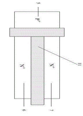
[0056] image 3 It is a horizontal SOI LDMOS structure diagram with a floating conventional n-type body region for comparison;

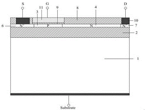
[0057] Figure 4 It is a schematic diagram of a lateral N-channel SOI LDMOS structure proposed by the present invention, in which the body region is drawn out through a silicon window.

[0058] Figure 4 The lateral N-channel SOI LDMOS structure in which the middle body region is drawn out through a silicon window includes: a semiconductor substrate 1 , an insulating dielectric layer 2 disposed on the semiconductor substrate 1 and a semiconductor active layer above the insulating dielectric layer 2 . The semiconductor substrate 1 , insulating dielectric layer 2 , and semiconductor active layer constitute SOI material, and a silicon window 13 is provided in the insulating dielectric layer 2 .

[0059] There are P-type body regions and N on the surface of the semiconductor active layer + drain region, the P-type body region and the N + There is a...

Embodiment 2

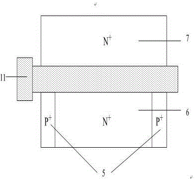
[0066] The structure of the semiconductor device of the present invention is described above by taking the lateral SOI LDMOS structure in which the N-channel body region is drawn out through the silicon window as an example, and the structure of the present invention is also applicable to the P-channel lateral SOI LDMOS. Such as Figure 5 shown in the lateral SOI LDMOS with Figure 4 The structure of the lateral SOI LDMOS corresponds to that, only the N-channel SOI LDMOS in Figure 4 is changed to the P-channel SOI LDMOS, so the conductivity type of each semiconductor region changes accordingly. In order to prevent the formation of a current path between the source and the substrate, only A P-type substrate can be used. However, the P-channel SOI LDMOS of the present invention is not suitable for integration with low-voltage SOI CMOS devices.

Embodiment 3

[0068]The structure of the semiconductor device of the present invention is described above by taking the lateral SOI LDMOS structure whose body region is drawn out through the silicon window as an example, and the structure of the present invention is also applicable to the lateral SOI LIGBT structure. Such as Figure 6 The lateral SOI IGBT structure shown with Figure 4 corresponding to the structure of the lateral SOI LDMOS, simply by Figure 4 The N-channel SOI LDMOS becomes an N-channel SOI LIGBT, so the conductivity type of the drain 7 changes accordingly. The N-channel SOI LIGBT of the invention can be well integrated with N-channel SOI LDMOS and low-voltage SOI CMOS devices on the same chip. P-channel SOI IGBT, like P-channel SOI LDMOS, is not suitable for integration with low-voltage SOI CMOS devices.


PUM


Abstract

The invention discloses a transverse signal operation instruction (SOI) power device. The transverse SOI power device comprises a semiconductor substrate, an insulating medium layer and a semiconductor active layer, wherein a body region and a drain region are arranged on the surface of the semiconductor active layer, an interval exists between the body region and the drain region to form a drift region of the device, a body contact region and a source region are sequentially formed on the surface of the body region, a silicon window is arranged on the insulating medium layer, the bottom of the body region is located in the silicon window or enters into the semiconductor substrate through the silicon window, the bottom of the body contact region enters into the silicon window, and a common leading-out end of the source region and the body contact region serves as a source electrode. The transverse SOI power device has the advantages that the body region is effectively led out, floating body effects of a Kink effect, a parasitic triode effect, memory effect and the like are eliminated, the off state withstand voltage and gate control capacity are improved, simultaneously the puncture voltage in an on state is boosted, characteristics of the SOI device are improved, and the possibility of a partial appendage effect appearing in a T-shaped gate structure and a base transceiver station (BTS) structure is eliminated.

Description

[0001] technical field [0002] The invention relates to the technical field of SOI semiconductor power devices and SOI intelligent power integrated circuits. Background technique [0003] The active layer of the SOI circuit is completely separated from the substrate, and between the high-voltage / low-voltage units by an insulating layer, while the active layer of the silicon-based circuit is directly electrically connected to the substrate, and the high-voltage and low-voltage units, the active layer and the The isolation between the substrate layers is accomplished by a reverse biased PN junction. Compared with bulk silicon technology, SOI technology has the advantages of high speed, low power consumption, high integration and easy isolation, etc., and weakens the latch-up effect and has strong anti-radiation ability, which makes the reliability and anti-software of SOI integrated circuits The failure capability is greatly improved. [0004] Smart power integrated circuit...

Claims


Application Information

Patent Timeline
Patent Type & Authority Applications(China)
IPC IPC(8): H01L29/06H01L29/41H01L27/088
Inventor 罗小蓉蒋永恒罗尹春范远航范叶王骁玮蔡金勇张波
Owner UNIV OF ELECTRONICS SCI & TECH OF CHINA
Why Eureka
Try Eureka