Method for manufacturing Cu (In, Ga) Se2 thin film of thin-film solar cell absorption layer
A technology for solar cells and absorbing layers, which is applied in coatings, circuits, electrical components, etc., can solve the problems of affecting the photoelectric conversion efficiency of cells, and the difficulty of achieving V-shaped structure distribution in the radial gradient of Ga concentration, so as to improve the utilization rate of raw materials, The effect of low scattering and mature technology
- Summary
- Abstract
- Description
- Claims
- Application Information
AI Technical Summary
Problems solved by technology
Method used
Image
Examples
Embodiment 1
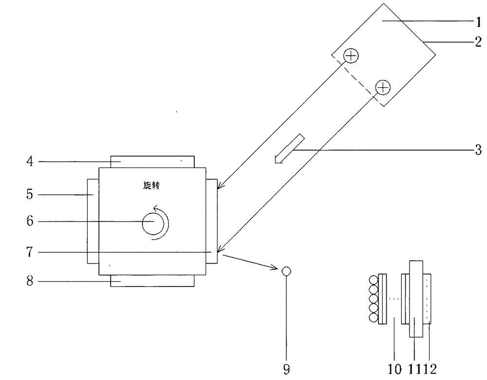
[0029] see figure 1 , figure 1 It is a schematic diagram of ion beam sputtering deposition of CIGS thin film. In the figure, 1 represents Ar plasma; 2 represents ion source; 3 represents sputtering ion beam; 4 represents Cu target; 5 represents In target; 6 represents multi-station rotary target holder; 7 represents Cu x Ga 1-x Target; 8 represents Se target; 9 represents sputtered atoms; 10 represents CIGS thin film; 11 represents coating substrate; 12 represents heating source.
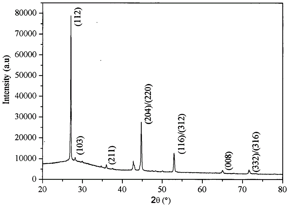
[0030] Cu, In, Se and CuGa (1:1) targets with a purity of 99.99% were respectively fixed on a four-station target frame; BK7 optical glass was used as the substrate, and organic solvent ultrasonic waves and auxiliary ion source sputtering were used for cleaning ; The background vacuum of the sputtering system was pumped to 8.0×10 -4 Pa, the inlet flow rate is 8sccm high-purity Ar gas, and the working pressure is controlled at 6.0×10 -2 Pa; accurate control of ion source parameters: plasma energ...
Embodiment 2
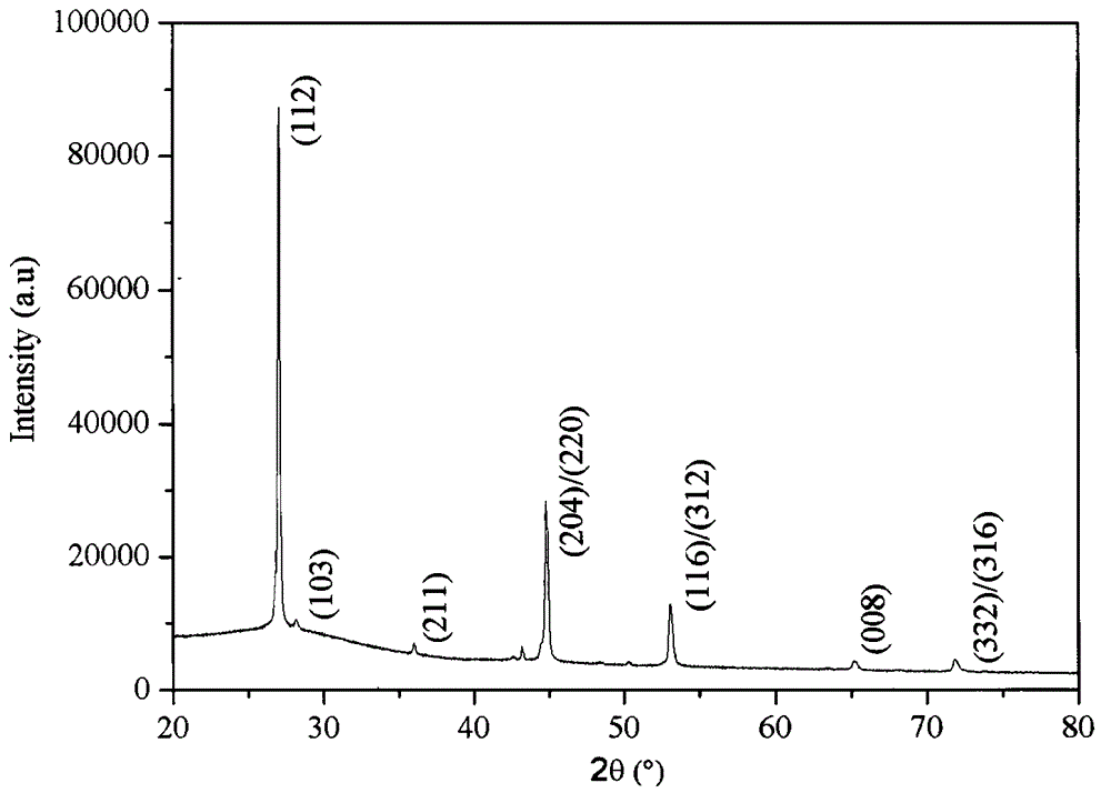
[0033] The difference from Example 1 is that the in-situ substrate temperature is raised to 550°C for heat treatment, such as image 3 The shown XRD pattern shows that the prepared CIGS film presents a single chalcopyrite structure, and the surface morphology of the film is as follows: Figure 4 As shown, it can be seen that the grain size of the film growth is larger and has a higher degree of crystallinity.
Embodiment 3
[0035] The difference from Example 1 is that the dual-period precursor thin film is prepared by ion beam sputtering, and its dual-period laminated structure is CuGa / Cu / In / Se / CuGa / Cu / In / Se. After heat treatment, the resulting thin film has a thickness of about A CIGS film with a thickness of 2 μm also produces a CIGS film with better structure and performance.
[0036] In summary, the thin film solar cell absorber layer Cu(In, Ga)Se of the present invention 2The preparation method of the thin film, which adopts the ion beam sputtering deposition method, in the same vacuum environment, high temperature in situ heat treatment ion beam sputtering precursor thin film stack or periodic stack to directly prepare the Cu(In, Ga)Se 2 film. Such as Figure 5 Shown, above-mentioned preparation method specifically comprises the following steps:
[0037] S1, high-purity Cu, In, Se and Cu x Ga 1-x The alloy is placed as a sputtering target on a multi-station turntable of an ion beam spu...
PUM
| Property | Measurement | Unit |
|---|---|---|
| Carrier concentration | aaaaa | aaaaa |
| Resistivity | aaaaa | aaaaa |
Abstract
Description
Claims
Application Information


