A kind of preparation method of cu(in,ga)se2 film of absorbing layer of thin film solar cell

A technology for solar cells and absorbing layers, applied to coatings, circuits, electrical components, etc., can solve the problems of affecting the photoelectric conversion efficiency of cells, and the difficulty of achieving V-shaped structure distribution with radial gradients of Ga concentration, so as to improve the utilization rate of raw materials, Effects for low scatter, improving quality and performance

Active Publication Date: 2016-01-06
SHENZHEN UNIV
View PDF3 Cites 0 Cited by
  • Summary
  • Abstract
  • Description
  • Claims
  • Application Information

AI Technical Summary

Problems solved by technology

The preparation of CIGS thin films by this method has certain advantages in reducing costs, improving material utilization, and realizing large-area preparation. However, since the metal prefabricated layer needs to be post-selenized in a special selenization furnace, it cannot be processed without breaking the vacuum. The next CIGS thin film will be completed, and there is still a technical problem, that is, during the high-temperature selenization process, Ga is easy to form an amorphous accumulation with the Mo electrode, and cannot be completely combined with Se to form a CIGS thin film, and it is difficult to achieve a V-shaped radial gradient of Ga concentration. Structural distribution, which affects the photoelectric conversion efficiency of the battery

Method used


Image

  • A kind of preparation method of cu(in,ga)se2 film of absorbing layer of thin film solar cell
  • A kind of preparation method of cu(in,ga)se2 film of absorbing layer of thin film solar cell
  • A kind of preparation method of cu(in,ga)se2 film of absorbing layer of thin film solar cell

Examples


Embodiment 1

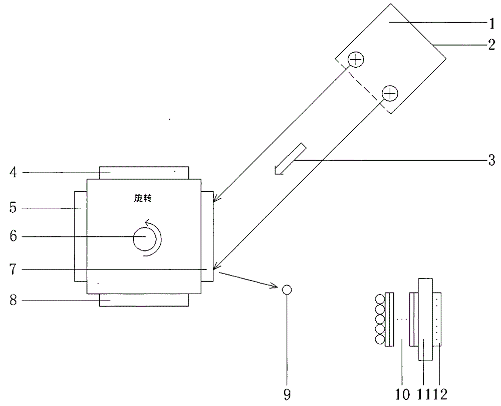
[0029] see figure 1 , figure 1 It is a schematic diagram of ion beam sputtering deposition of CIGS thin film. In the figure, 1 represents Ar plasma; 2 represents ion source; 3 represents sputtering ion beam; 4 represents Cu target; 5 represents In target; 6 represents multi-station rotary target holder; 7 represents Cu x Ga 1-x Target; 8 represents Se target; 9 represents sputtered atoms; 10 represents CIGS thin film; 11 represents coating substrate; 12 represents heating source.

[0030] Cu, In, Se and CuGa (1:1) targets with a purity of 99.99% were respectively fixed on a four-station target frame; BK7 optical glass was used as the substrate, and organic solvent ultrasonic waves and auxiliary ion source sputtering were used for cleaning ; The background vacuum of the sputtering system was pumped to 8.0×10 -4 Pa, the inlet flow rate is 8sccm high-purity Ar gas, and the working pressure is controlled at 6.0×10 -2 Pa; accurate control of ion source parameters: plasma energ...

Embodiment 2

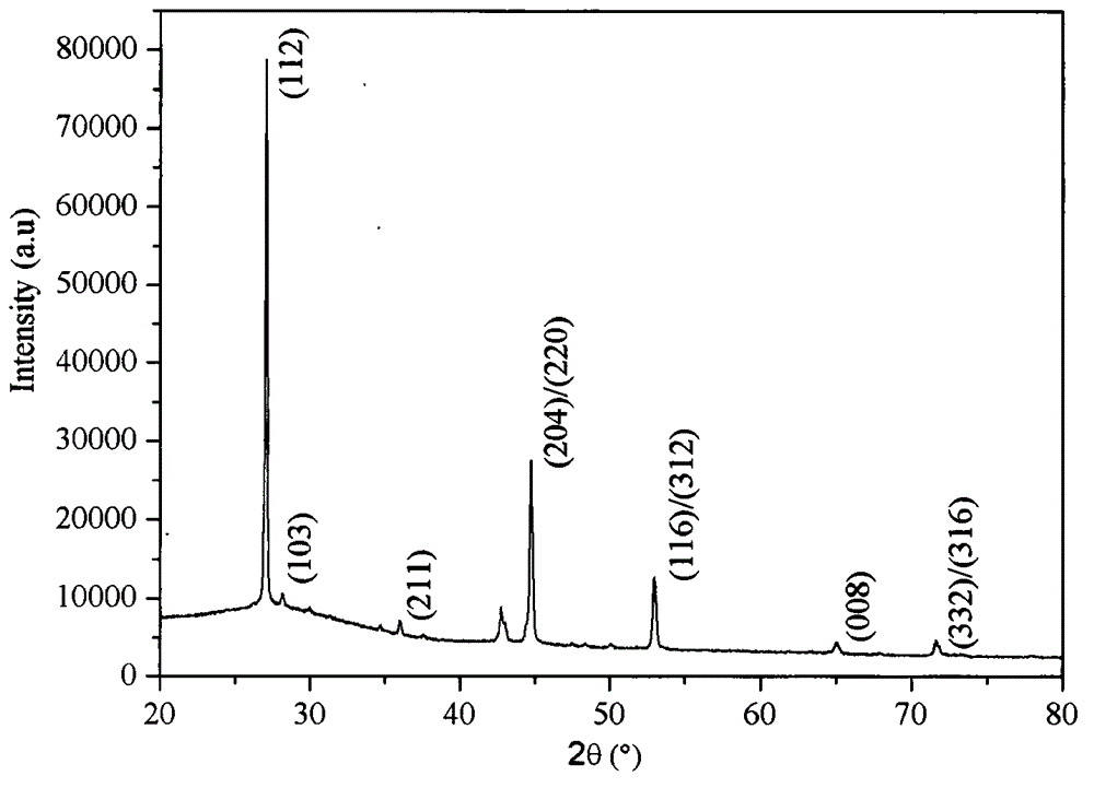
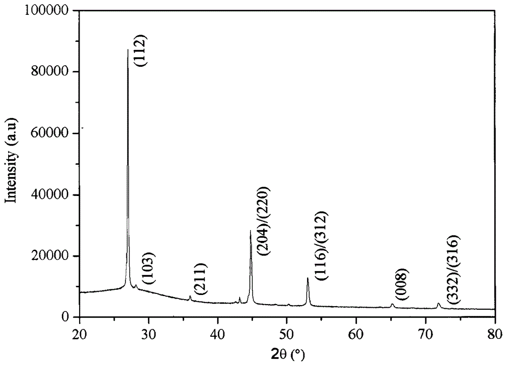
[0033] The difference from Example 1 is that the in-situ substrate temperature is raised to 550°C for heat treatment, such as image 3 The shown XRD pattern shows that the prepared CIGS film presents a single chalcopyrite structure, and the surface morphology of the film is as follows: Figure 4 As shown, it can be seen that the grain size of the film growth is larger and has a higher degree of crystallinity.

Embodiment 3

[0035] The difference from Example 1 is that the dual-period precursor thin film is prepared by ion beam sputtering, and its dual-period laminated structure is CuGa / Cu / In / Se / CuGa / Cu / In / Se. After heat treatment, the resulting thin film has a thickness of about A CIGS film with a thickness of 2 μm also produces a CIGS film with better structure and performance.

[0036] In summary, the thin film solar cell absorber layer Cu(In, Ga)Se of the present invention 2 The preparation method of the thin film, which adopts the ion beam sputtering deposition method, in the same vacuum environment, high temperature in situ heat treatment ion beam sputtering precursor thin film stack or periodic stack to directly prepare the Cu(In, Ga)Se2 film. Such as Figure 5 Shown, above-mentioned preparation method specifically comprises the following steps:

[0037] S1, high-purity Cu, In, Se and Cu x Ga 1-x The alloy is placed as a sputtering target on a multi-station turntable of an ion beam sput...


PUM


Abstract

The invention discloses a novel method for manufacturing Cu (In, Ga) Se2 thin film of a thin-film solar cell absorption layer. The method includes steps of employing a method of ion beam sputtering deposition, taking high-purity Cu, In, Se and an alloy of CuxGa1-x as sputtering target materials, successively sputtering elements or alloy target materials to manufacture a precursor thin-film lamination or periodic lamination thin film by accurately controlling ion beam sputtering parameters, and manufacturing the Cu (In, Ga) Se2 thin film by means of high-temperature in-situ heat treatment in the same vacuum environment. The method for manufacturing Cu (In, Ga) Se2 thin film of the thin-film solar cell absorption layer is optimized in doping process, simple in operation and capable of improving a utilization ratio of raw materials, realizing doping of the Ga element on the basis of the Cu (In, Ga) Se2 thin films and effectively controlling radial distribution of the Ga element. The structure and performance of the Cu (In, Ga) Se2 thin film manufactured by the method can meet performance requirements of high-efficient photovoltaic devices, and a new way is explored for development and utilization of the solar cell.

Description

technical field [0001] The invention relates to the field of photoelectric functional materials, in particular to a Cu(In, Ga)Se absorbing layer of a thin-film solar cell 2 The method of film preparation. Background technique [0002] Copper indium selenide thin film solar cells are based on polycrystalline CuInSe 2 (CIS) thin film is the solar cell of the absorber layer. On the basis of the CIS thin film, the metal Ga element is used to partially replace the In element to achieve doping, which is called copper indium gallium selenide Cu(In,Ga)Se 2 (CIGS) thin film solar cells. In order to absorb the solar spectrum optimally, the optimal bandgap of solar cell materials should be about 1.45eV, but the bandgap of CIS thin film materials at room temperature is only 1.02eV, which is not the best bandgap structure. Therefore, by doping a certain concentration of Ga, a CIGS thin film material is prepared. Studies have shown that using the CIGS thin film as an absorber layer can...

Claims


Application Information

Patent Timeline
Patent Type & Authority Patents(China)
IPC IPC(8): H01L31/18C23C14/06C23C14/34
CPCY02P70/50
Inventor 范平梁广兴曹鹏举郑壮豪
Owner SHENZHEN UNIV
Why Eureka
Try Eureka