Method for manufacturing thin line with relatively small edge roughness

A technology with edge roughness and thin lines, applied in the field of VLSI manufacturing, it can solve the problems of lack of advantages, limited development, and long time-consuming, and achieve the effect of short process time, strong operability, and LER improvement.

Inactive Publication Date: 2012-11-07
PEKING UNIV
View PDF7 Cites 5 Cited by
  • Summary
  • Abstract
  • Description
  • Claims
  • Application Information

AI Technical Summary

Problems solved by technology

[0003] Although electron beam lithography can be used to prepare thin lines, it has no advantages in industrial production due to long time consumption and high cost, and electron scattering exists in electron beam lithography engineering, so it is a great challenge to prepare thin lines below 30nm
Other preparation methods, such as ordinary photolithography and oxidation process, although thin lines can be prepared, but the thin lines have a large LER (edge ​​roughness), and oxidation requires high-temperature processing, which takes a long time and high cost, which limits its development in industrial production

Method used


Image

  • Method for manufacturing thin line with relatively small edge roughness
  • Method for manufacturing thin line with relatively small edge roughness
  • Method for manufacturing thin line with relatively small edge roughness

Examples


preparation example Construction

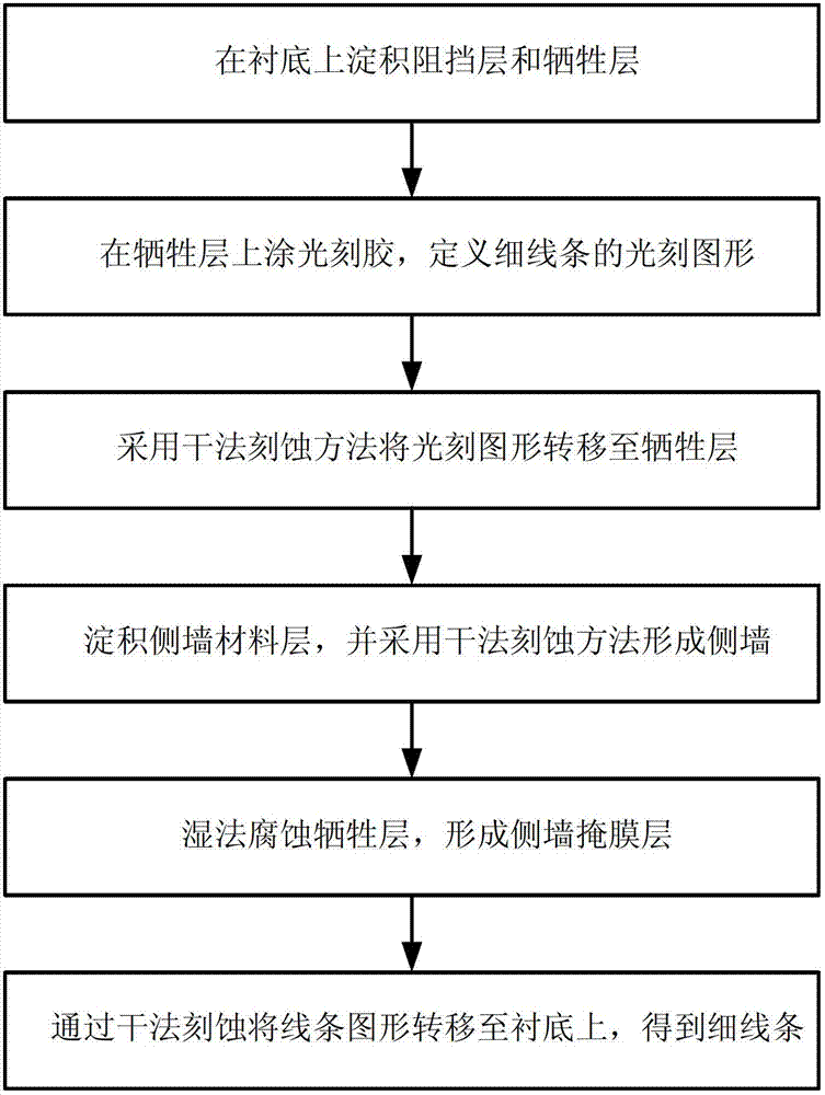
[0029] figure 1 It is a flow chart of the steps of the method for preparing thin lines with less edge roughness in this embodiment. The process can be further summarized into the following three major steps:

[0030] 1) Deposit a barrier layer and a sacrificial layer on the substrate, and define the lithographic pattern of the lines.

[0031] The material of the blocking layer is silicon oxide, which acts as a blocking layer of the substrate during the subsequent etching of the sacrificial layer and etching of the sacrificial layer. The material of the sacrificial layer is polysilicon, which serves as a support layer for subsequent deposition of side walls. The specific process steps include:

[0032] a) Depositing a barrier layer of silicon oxide to block subsequent etching and corrosion;

[0033] b) depositing a layer of polysilicon film;

[0034] c) Coating a layer of photoresist on the polysilicon, and defining thin lines by photolithography;

[0035] d) Dry etching ...

Embodiment 1

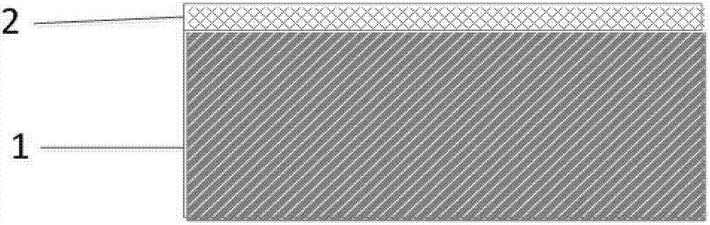
[0049] 1. Chemical vapor deposition of a silicon oxide film on a (100) / bulk silicon substrate with a thickness of As shown in Figure 2(a).

[0050] 2. Chemical vapor deposition of a layer of polysilicon film on the silicon oxide film with a thickness of As shown in Figure 2(b);

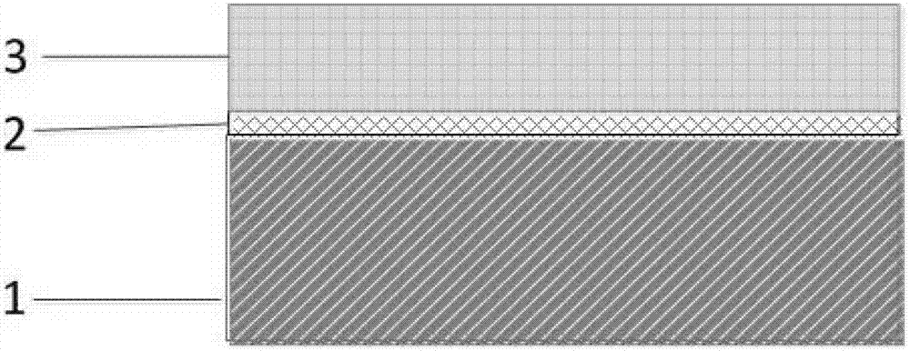
[0051] 3. Coating photoresist on the polysilicon film, as shown in Figure 2(c);

[0052] 4. Photolithography defines the area to be used as the sacrificial layer, as shown in Figure 2(d);

[0053] 5. Anisotropic dry etching of the polysilicon film, and finally transfer the pattern on the photoresist to the polysilicon film material, as shown in Figure 2(e);

[0054] 6. Remove the photoresist, as shown in Figure 2(f);

[0055] 7. Chemical vapor deposition of silicon nitride on the surface of silicon oxide film and polysilicon film, with a thickness of As shown in Figure 2(g);

[0056] 8. Anisotropic dry etching of silicon nitride to form silicon nitride sidewalls, as shown in Figure 2(h);

...

Embodiment 2

[0063] This example provides process parameters for producing thinner lines with smaller dimensions. To produce thinner lines with smaller dimensions, the thickness of the polysilicon sacrificial layer can be increased. In this way, when silicon nitride is etched to form sidewalls, the size of the silicon nitride hard mask is smaller due to the more serious lateral undercutting, and the size of the finally prepared thin lines is also smaller, which can reach below 10nm. Specific steps are as follows:

[0064] 1. Chemical vapor deposition of a silicon oxide film on a (100) / bulk silicon substrate with a thickness of As shown in Figure 2(a).

[0065] 2. Chemical vapor deposition of a layer of polysilicon film on the silicon oxide film with a thickness of As shown in Figure 2(b);

[0066] 3. Coating photoresist on the polysilicon film, as shown in Figure 2(c);

[0067] 4. Photolithography defines the area to be used as the sacrificial layer, as shown in Figure 2(d);

[00...


PUM

PropertyMeasurementUnit
sizeaaaaaaaaaa

Abstract

The invention provides a method for manufacturing a thin line with relatively small edge roughness, comprising the following steps of depositing a blocking layer and a sacrificial layer on a substrate; coating photoresist on the sacrificial layer, and defining a photoetching graph of the line; transferring the photoetching graph to the sacrificial layer by using a dry etching method; depositing a side wall material layer, and forming a side wall by using the dry etching method; carrying out wet etching on the sacrificial layer in the side wall to form a side wall mask layer; and transferring the line graph to the substrate by using the side wall mask layer and through the dry etching method, so as to obtain the thin line. The method disclosed by the invention is combined with the side wall technology and the wet etching technology; electron-beam lithography, high-temperature oxidation and the like are not used; and the thin line with small edge roughness can be obtained.

Description

technical field [0001] The invention belongs to the technical field of ultra-large-scale integrated circuit manufacturing, and relates to a method for preparing ultra-thin lines in integrated circuits, in particular to a method for preparing ultra-thin lines with small edge roughness by combining side wall technology and wet etching. Background technique [0002] With the development of integrated circuits and the continuous improvement of the integration level of devices, the size of devices is required to be continuously reduced, and the preparation of small-sized thin lines is becoming more and more critical. [0003] Although electron beam lithography can be used to prepare thin lines, it has no advantages in industrial production due to long time consumption and high cost, and electron scattering exists in electron beam lithography engineering, so it is a great challenge to prepare thin lines below 30nm. Other preparation methods, such as ordinary photolithography and o...

Claims


Application Information

Patent Timeline
Patent Type & Authority Applications(China)
IPC IPC(8): H01L21/311
Inventor 黄如李佳黎明张耀凯许晓燕
Owner PEKING UNIV
Why Eureka
Try Eureka