

Preparation method for low excursion flat belt voltage silicon carbide (SiC) metal oxide semiconductor (MOS) capacitance
A technology of flat-band voltage and manufacturing method, which is applied in the field of microelectronics, can solve problems such as difficult nitrogen-containing gas dosage, influence on device interface characteristics, flat-band voltage offset, etc., and achieve reduction of dangling bonds, ease of interface stress, and flat-band voltage The effect of small offset
- Summary
- Abstract
- Description
- Claims
- Application Information
AI Technical Summary
Problems solved by technology
Method used
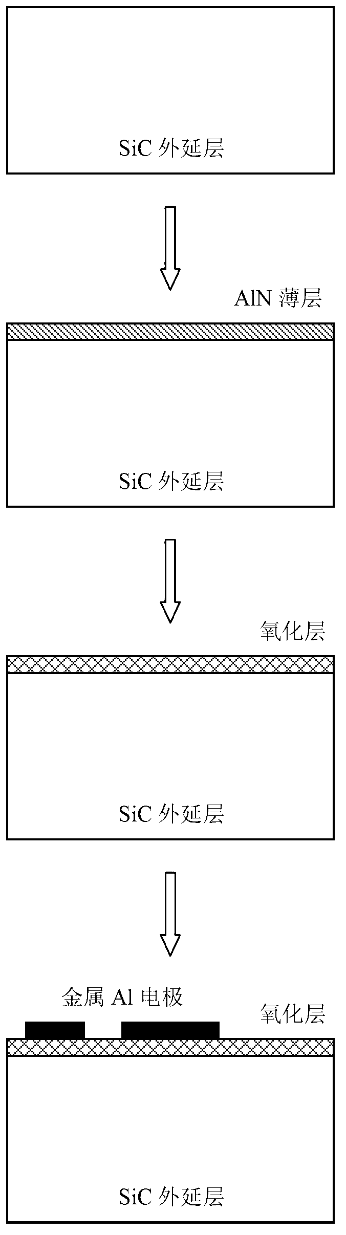
Image

Examples
Embodiment 1
[0019] Embodiment 1, comprises the steps:
[0020] Step 1, perform standard cleaning treatment on the N-SiC epitaxial material:
[0021] 1.1) Ultrasonic cleaning of N-SiC epitaxial materials with deionized water;
[0022] 1.2) Clean with concentrated sulfuric acid, heat to smoke, cook for 10 minutes, soak for 30 minutes, and rinse the surface with deionized water several times;
[0023] 1.3) Use H in a ratio of 5:1:1 2 O, H 2 o 2 Soak the N-SiC epitaxial material washed with deionized water in a water bath for 5 minutes in the No. 1 mixed liquid composed of ammonia water at a temperature of 80°C, then wash it with hydrogen fluoride solution, and rinse the surface several times with deionized water for the second time ;
[0024] 1.4) Use H with a ratio of 6:1:1 2 O, H 2 o 2 In the No. 2 mixed liquid composed of HCl at a temperature of 80°C, soak the N-SiC epitaxial material after the second rinse with deionized water in a water bath for 5 minutes, wash it with hydrogen ...
Embodiment 2
[0029] Embodiment 2, comprises the steps:
[0030] Step 1, perform standard cleaning treatment on the N-SiC epitaxial material:
[0031] 1.1) Ultrasonic cleaning of N-SiC epitaxial materials with deionized water;
[0032] 1.2) Clean with concentrated sulfuric acid, heat to smoke, cook for 10 minutes, soak for 30 minutes, and rinse the surface with deionized water several times;
[0033] 1.3) Use H in a ratio of 5:1:1 2 O, H 2 o 2 Soak the N-SiC epitaxial material washed with deionized water in a water bath for 5 minutes in the No. 1 mixed liquid composed of ammonia water at a temperature of 80°C, then wash it with hydrogen fluoride solution, and rinse the surface several times with deionized water for the second time ;
[0034] 1.4) Use H with a ratio of 6:1:1 2 O, H 2 o 2 In the No. 2 mixed liquid composed of HCl at a temperature of 80°C, soak the N-SiC epitaxial material after the second rinse with deionized water in a water bath for 5 minutes, wash it with hydrogen ...
Embodiment 3
[0039] Embodiment 3, comprises the steps:
[0040] Step 1, perform standard cleaning treatment on the N-SiC epitaxial material:
[0041] 1.1) Ultrasonic cleaning of N-SiC epitaxial materials with deionized water;
[0042] 1.2) Clean with concentrated sulfuric acid, heat to smoke, cook for 10 minutes, soak for 30 minutes, and rinse the surface with deionized water several times;
[0043] 1.3) Use H in a ratio of 5:1:1 2 O, H 2 o 2Soak the N-SiC epitaxial material washed with deionized water in a water bath for 5 minutes in the No. 1 mixed liquid composed of ammonia water at a temperature of 80°C, then wash it with hydrogen fluoride solution, and rinse the surface several times with deionized water for the second time ;
[0044] 1.4) Use H with a ratio of 6:1:1 2 O, H 2 o 2 In the No. 2 mixed liquid composed of HCl at a temperature of 80°C, soak the N-SiC epitaxial material after the second rinse with deionized water in a water bath for 5 minutes, wash it with hydrogen f...
PUM
| Property | Measurement | Unit |
|---|---|---|
| Thickness | aaaaa | aaaaa |
| Diameter | aaaaa | aaaaa |
| Diameter | aaaaa | aaaaa |
Abstract
Description
Claims
Application Information