

Manufacturing method of high-voltage quick-recovery diode
A technology of rapid recovery and manufacturing method, applied in the direction of semiconductor/solid-state device manufacturing, electrical components, circuits, etc., can solve the problems of high manufacturing cost, cumbersome steps, long manufacturing period, etc., to reduce costs, reduce processing steps, and remove damage. and the tainted effect
- Summary
- Abstract
- Description
- Claims
- Application Information
AI Technical Summary
Problems solved by technology
Method used
Image


Examples
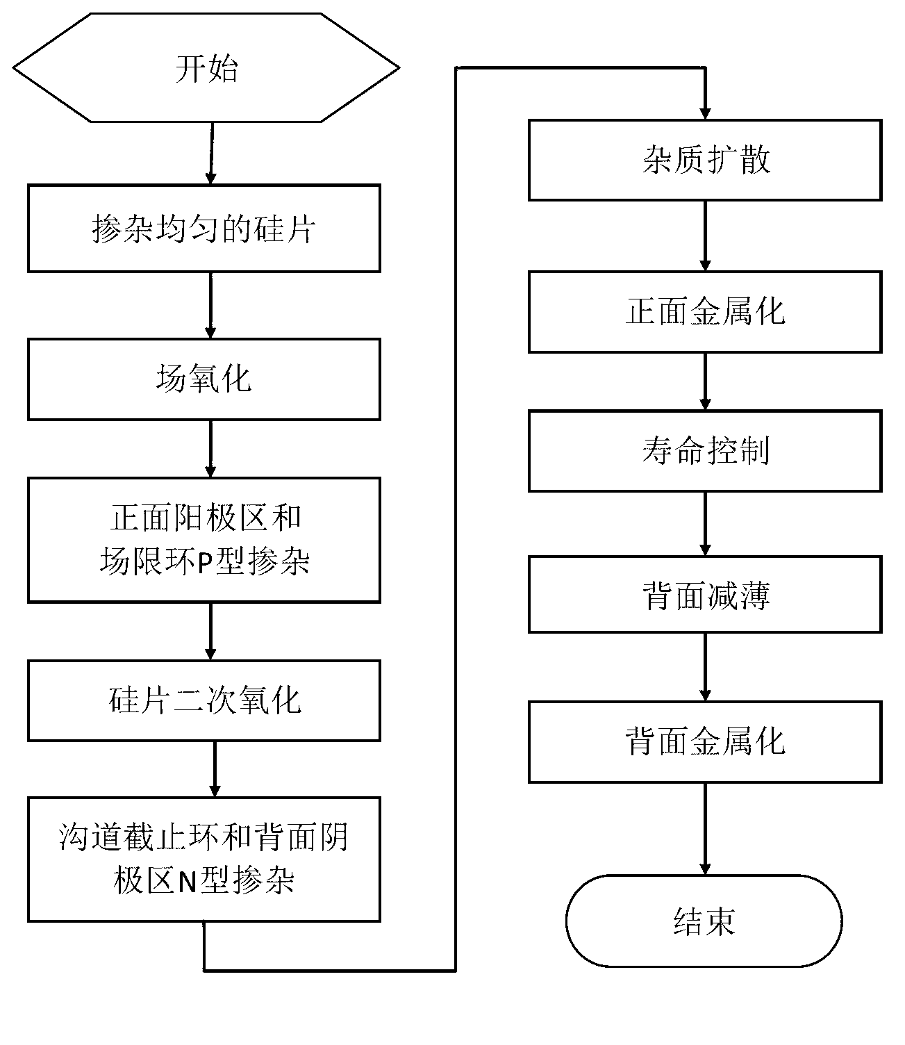
Embodiment 1
[0038] Embodiment 1 The manufacturing method of the fast recovery diode of the present invention includes the following 8 process modules:
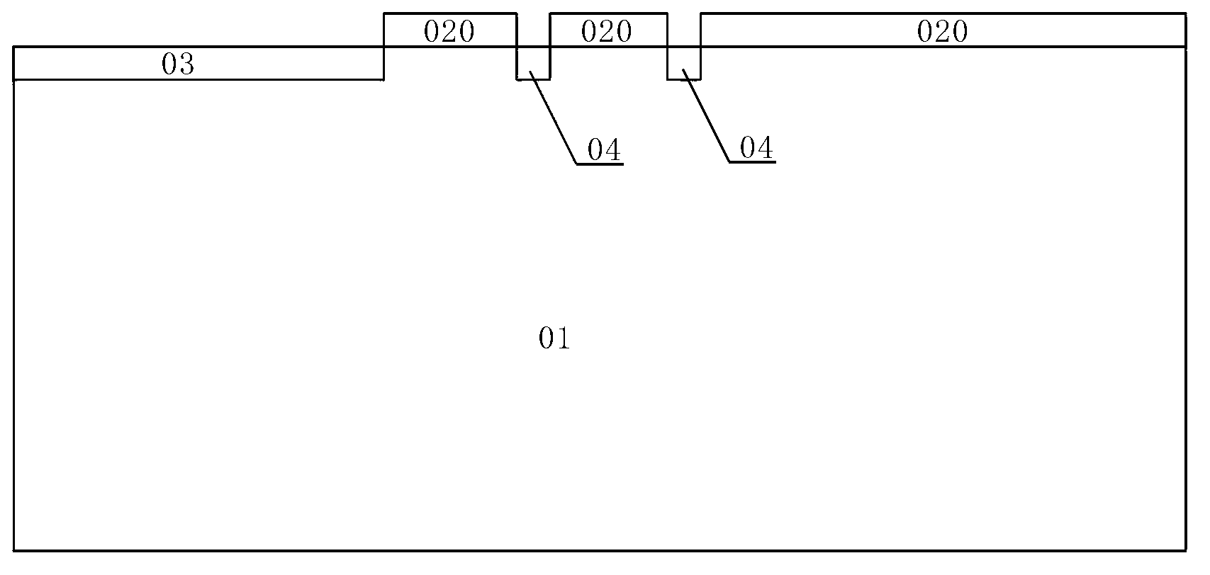
[0039] 1. After cleaning the uniformly doped N-type single crystal silicon wafer 01, oxidize it at high temperature, and grow a layer of 1-4um oxide film 020 on the surface of the silicon wafer, such as figure 2 shown.
[0040] 2. After gluing, exposure, development, oxide film etching, and degumming, etc., the window doped with P-type impurities is carved out, and P-type impurities are doped with aluminum or boron ion implantation, such as image 3 As shown, two types of P-type doped regions of FRD are formed: the anode region doped layer 03 and the terminal field limiting ring 04, and the implantation dose is 2×10 12 ~2×10 14 / cm 2 .
[0041] 3. After the silicon wafer is cleaned again, a layer of 1-4um oxide layer 022 is grown on the surface of the silicon wafer by high-temperature oxidation to protect the area other than the N-ty...
Embodiment 2
[0048] The second implementation mode is to do the N-type impurity doping first and then do the P-type impurity doping. The steps are as follows: Figure 9 Shown, specific process module is similar to embodiment 1.
PUM
 Abstract
Description
Claims
Application Information