A method for surface treatment of crystalline silicon wafers

A technology of crystalline silicon wafer and single crystal silicon wafer, which is applied in the manufacture of semiconductor/solid-state devices, electrical components, circuits, etc. Problems such as falling conversion rates

Active Publication Date: 2015-09-09
SHARESUN CO LTD
View PDF4 Cites 0 Cited by
  • Summary
  • Abstract
  • Description
  • Claims
  • Application Information

AI Technical Summary

Problems solved by technology

In other words, cast monocrystalline silicon wafers will produce a large contrast of reflected light after being textured by alkaline solution, which seriously affects the appearance of solar cell modules produced by cast monocrystalline silicon wafer solar cells
[0011] If the traditional polycrystalline silicon wafer texturing method is adopted, that is, the acid solution texturing method is used to texture the cast single crystal silicon wafer, although the difference in reflectivity between the single crystal silicon area and the polycrystalline silicon area can be greatly improved, but due to the As the reflectivity of the silicon region increases, the photoelectric conversion rate of the monolithic cast monocrystalline silicon solar cell also decreases.

Method used


Image

  • A method for surface treatment of crystalline silicon wafers
  • A method for surface treatment of crystalline silicon wafers
  • A method for surface treatment of crystalline silicon wafers

Examples


Embodiment 1

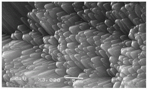
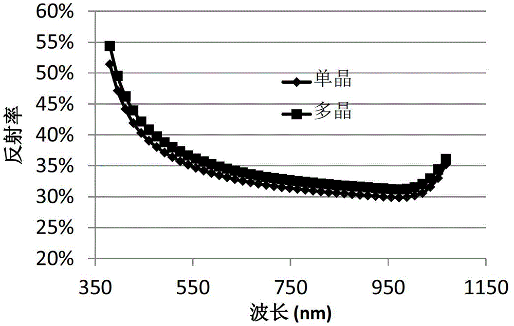
[0071] A 20% by weight tetramethyl ammonium hydroxide solution is used as the etching and polishing solution, and the etching and polishing solution is heated to 90 degrees for use. Configure 1.5% by weight sodium hydroxide solution as the corrosion texturing solution, heat the corrosion texturing to 78 degrees, add appropriate amount of isopropanol and texturing additives for later use. Put the cast monocrystalline silicon wafer containing 30% polycrystalline silicon area into the etching and polishing solution. After 5 minutes, the cast monocrystalline silicon wafer was taken out of the etching and polishing solution, and then put into the etching and texturing solution. After 7 minutes of texturing, take it out and wash with deionized water. The average reflectivity in the monocrystalline silicon region was 9.9%, and the average reflectivity in the polycrystalline silicon region was 18%. The cast monocrystalline silicon wafer was prepared into a solar cell, and the photoel...

Embodiment 2

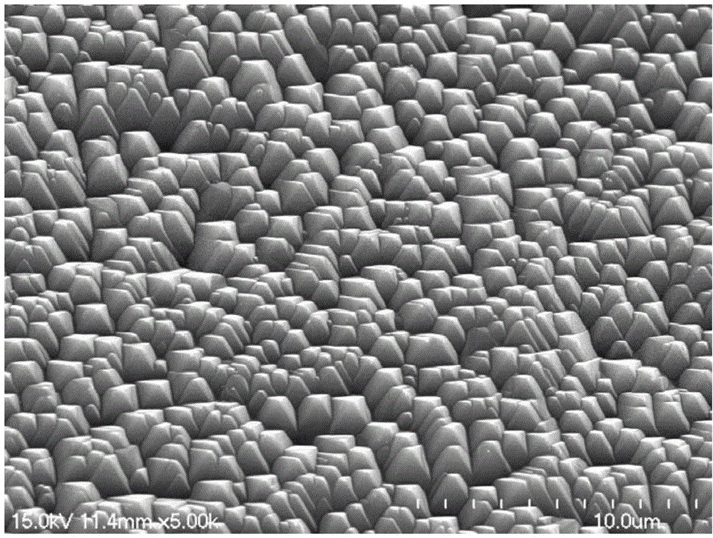
[0073] A mixed solution of 20% by weight of hydrofluoric acid, 45% by weight of nitric acid and 20% by weight of acetic acid was prepared as the corrosion polishing solution, and the temperature of the corrosion polishing solution was kept at 5 degrees for use. Prepare 1.5% by weight potassium hydroxide solution as the corrosive texturing solution, heat the corrosive texturing solution to 75 degrees and add appropriate amount of texturing additives for later use. Put the polysilicon wafer into the etching and polishing solution. The polycrystalline silicon wafer was taken out of the etching and polishing solution after 2 minutes, washed with deionized water, and put into the etching and texturing solution. Take it out after 10 minutes of texturing and wash it with deionized water. The measured average reflectivity is 19%. The polycrystalline silicon wafer was prepared into a solar cell, and the photoelectric conversion efficiency of the solar cell was measured to be 16.8%. Th...

Embodiment 3

[0075] A 5% weight percent sodium hydroxide solution is used as the corrosion polishing solution, and the corrosion polishing solution is heated to 85 degrees for use. Configure 2% tetramethyl ammonium hydroxide solution as the corrosive texturing solution, heat the corrosive texturing to 80 degrees, add appropriate amount of isopropanol and texturing additives for later use. Put the monocrystalline silicon wafer into the etching and polishing solution. The monocrystalline silicon wafer was taken out of the etching and polishing solution after 3 minutes, and directly put into the etching and texturing solution. After 5 minutes of texturing, take it out and wash with deionized water. The average reflectivity of the single crystal silicon wafer was 10.1%. The monocrystalline silicon wafer was prepared into a solar cell, and the photoelectric conversion efficiency of the solar cell was measured to be 18.4%, in which the open circuit voltage, short circuit current and quality fac...


PUM

PropertyMeasurementUnit
surface roughnessaaaaaaaaaa
reflectanceaaaaaaaaaa

Abstract

The invention discloses a woolen making method of a crystal wafer. The woolen making method comprises the steps of: (1) carrying out isotropic etching polishing of chemical solution on the surface of the crystal wafer, reducing the surface roughness of the crystal wafer, (2) carrying out isotropic etching woolen making treatment of the chemical solution on the surface of the crystal wafer, and reducing the surface reflectance of the crystal wafer. The woolen making method is characterized in that the woolen making method is suitable for all types of crystal wafers, and is small in woolen surface, low in production cost and short in woolen making time.

Description

technical field [0001] The invention relates to a method for treating the surface of a crystalline silicon wafer in the process of producing a solar cell, in particular to a technique for preparing a textured surface on the surface of a crystalline silicon wafer. The surface treatment technology of the present invention has the advantages of wide applicability, small suede size, low production cost, short time for making suede, and the like. Background technique [0002] As the known non-renewable energy sources on the earth, such as coal, oil, etc., continue to decrease, the development and utilization of renewable energy sources have attracted more and more attention. Solar cell technology, which converts solar energy into electrical energy, is one of the main technologies for renewable energy utilization at present. Among them, crystalline silicon solar cells are the most widely used solar cells among various solar cell technologies. [0003] Crystalline silicon solar c...

Claims


Application Information

Patent Timeline
Patent Type & Authority Patents(China)
IPC IPC(8): H01L21/306
Inventor 季静佳覃榆森朱凡
Owner SHARESUN CO LTD
Why Eureka
Try Eureka