Germanium-base substrate surface passivation method

A substrate surface and substrate technology, which is applied in the manufacture of electrical components, circuits, semiconductors/solid-state devices, etc., can solve the problems of reducing the interface state and cannot effectively suppress the diffusion and thinning of germanium surface atoms, so as to reduce the interface state Effect

Active Publication Date: 2013-01-30
PEKING UNIV
View PDF4 Cites 3 Cited by
  • Summary
  • Abstract
  • Description
  • Claims
  • Application Information

AI Technical Summary

Problems solved by technology

One is to use H passivation and Cl passivation in traditional silicon technology to passivate the surface dangling bonds to reduce the interface state, but studies have shown that the passivation effect of this method, such as the formation of Ge-H, Ge-Cl bond chemistry Poor stability, easy to break, unable to effectively suppress the outdiffusion of germanium surface atoms
The second is to insert an ultra-thin layer at the interface between the germanium substrate and the gate dielectric, which can be a dielectric or a semiconductor epitaxial layer, such as SiO 2 、GeO x N y , Si, etc., but this method is not conducive to the reduction of the equivalent gate oxide thickness (EOT)

Method used


Image

  • Germanium-base substrate surface passivation method
  • Germanium-base substrate surface passivation method
  • Germanium-base substrate surface passivation method

Examples


Embodiment Construction

[0021] The method of the present invention will be further described through specific embodiments below in conjunction with the accompanying drawings and the germanium substrate.

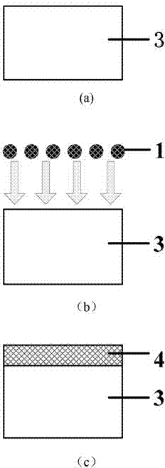
[0022] 1) Clean the germanium substrate and remove the surface oxide layer, such as image 3 as shown in (a);

[0023] 2) Put the cleaned germanium substrate into the inductively coupled plasma chamber, use the reactive gas to generate plasma and process the germanium sheet in a plasma bath, and apply RIE power while the plasma bath is being processed.

[0024] The reaction gas can be an elemental gas corresponding to a multibond atom and / or a hydride containing a multibond atom, or one or more gases and inert gas in the elemental gas corresponding to a multibond atom and a hydride containing a multibond atom Mixed gas of atomic gas (such as Ar gas). This embodiment preferably uses N 2 Mix gas with Ar to generate nitrogen plasma, and conduct plasma bath treatment on germanium substrates, such as ...


PUM


Abstract

The invention discloses a germanium-base substrate surface passivation method, which comprises the following steps of: cleaning a surface of a germanium-base substrate; putting the cleaned germanium-base substrate into a plasma cavity; utilizing reaction gas corresponding to multiply-bound atoms to generate a plasma; carrying out plasma bath processing on the surface of the germanium-base substrate; and applying a guiding electric field in a plasma bath processing process to guide the plasma to drift to the surface of the germanium-base substrate. Due to the processing, covalently joint of activated the multiply-bound atoms and germanium surface atoms is formed, but an interface layer containing germanium compounds is not generated, so that a surface dangling bond is passivated, the probability that the germanium surface atoms are separated from the surface of the germanium-base substrate to be dispersed is reduced, and simultaneously, the phenomenon that the thinning of the EOT is unfavorable as the interface layer is introduced is avoided. In addition, the guiding electric filed is applied, so that the formation of germanium oxides can be effectively suppressed, the passivation efficiency is improved, and the density of interfacial states is reduced.

Description

technical field [0001] The invention belongs to the field of semiconductor devices, and in particular relates to a semiconductor surface passivation method. Background technique [0002] As the silicon-based Metal-Oxide-Semiconductor Field-Effect Transistor (MOSFET) shrinks to the nanometer scale, the traditional method of improving performance and integration by reducing device size is facing the dual limit test of physics and technology. In order to further improve device performance, one of the effective methods is to introduce high-mobility channel materials. Due to the high electron and hole mobility at the same time (at room temperature (300K), the electron mobility of the germanium channel is 2.4 times that of silicon, and the hole mobility is 4 times that of silicon), germanium materials and germanium-based devices have become an option. [0003] At present, in the preparation technology of germanium-based MOS devices, the interface problem between the germanium su...

Claims


Application Information

Patent Timeline
Patent Type & Authority Applications(China)
IPC IPC(8): H01L21/3065
Inventor 黄如林猛云全新李敏王佳鑫安霞黎明张兴
Owner PEKING UNIV
Why Eureka
Try Eureka