Electron transfer layer, organic electroluminescent device with electron transfer layer and manufacturing method thereof
An electron transport layer, organic electronics technology, applied in semiconductor/solid-state device manufacturing, electrical solid-state devices, electrical components, etc. Good film formation, good thermal stability, long life effect
- Summary
- Abstract
- Description
- Claims
- Application Information
AI Technical Summary
Problems solved by technology
Method used
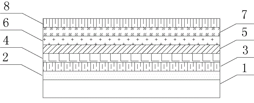
Image

Examples
Embodiment Construction
[0048] The present invention will be further described below in conjunction with the accompanying drawings and specific embodiments, so that those skilled in the art can better understand the present invention and implement it, but the examples given are not intended to limit the present invention.
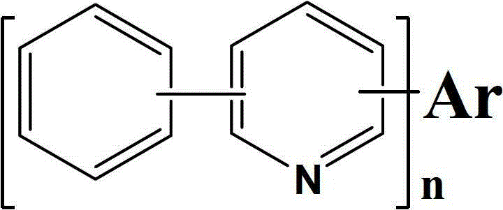
[0049] The electron transport layer of the present invention is a blended electron transport layer, containing an organic electron transport material and an organometallic complex, wherein the organic electron transport material is one of the compounds with the structure of formula I or any of two or more combination,
[0050]
[0051] Formula Ⅰ
[0052] In formula I, Ar is selected from condensed aromatic hydrocarbons with 6 to 30 carbon atoms, or selected from condensed heterocyclic aromatic hydrocarbons with 6 to 30 carbon atoms; n is selected from an integer of 1 to 3.
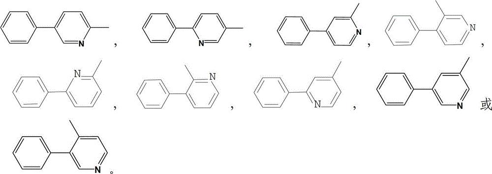
[0053] Specifically, the compound having the structure of formula I may be of the following structure: ...
PUM
| Property | Measurement | Unit |
|---|---|---|
| Thickness | aaaaa | aaaaa |
Abstract
Description
Claims
Application Information
 - Generate Ideas
- Intellectual Property
- Life Sciences
- Materials
- Tech Scout
- Unparalleled Data Quality
- Higher Quality Content
- 60% Fewer Hallucinations
Browse by: Latest US Patents, China's latest patents, Technical Efficacy Thesaurus, Application Domain, Technology Topic, Popular Technical Reports.
© 2025 PatSnap. All rights reserved.Legal|Privacy policy|Modern Slavery Act Transparency Statement|Sitemap|About US| Contact US: help@patsnap.com