

Method for manufacturing lateral double-diffused metal oxide semiconductor (LDMOS) device
A technology of substrate and metal silicide layer, which is applied in semiconductor/solid-state device manufacturing, electrical components, circuits, etc., can solve the problems of LDMOS on-resistance Rdson increase, LDMOS performance degradation, and channel length lengthening, etc., to simplify Process complexity, Peeling elimination, high performance effect
- Summary
- Abstract
- Description
- Claims
- Application Information
AI Technical Summary
Problems solved by technology
Method used
Image

Examples
Embodiment 1
[0042] Such as figure 1 As shown, a method for manufacturing an LDMOS device provided by an embodiment of the present invention includes:
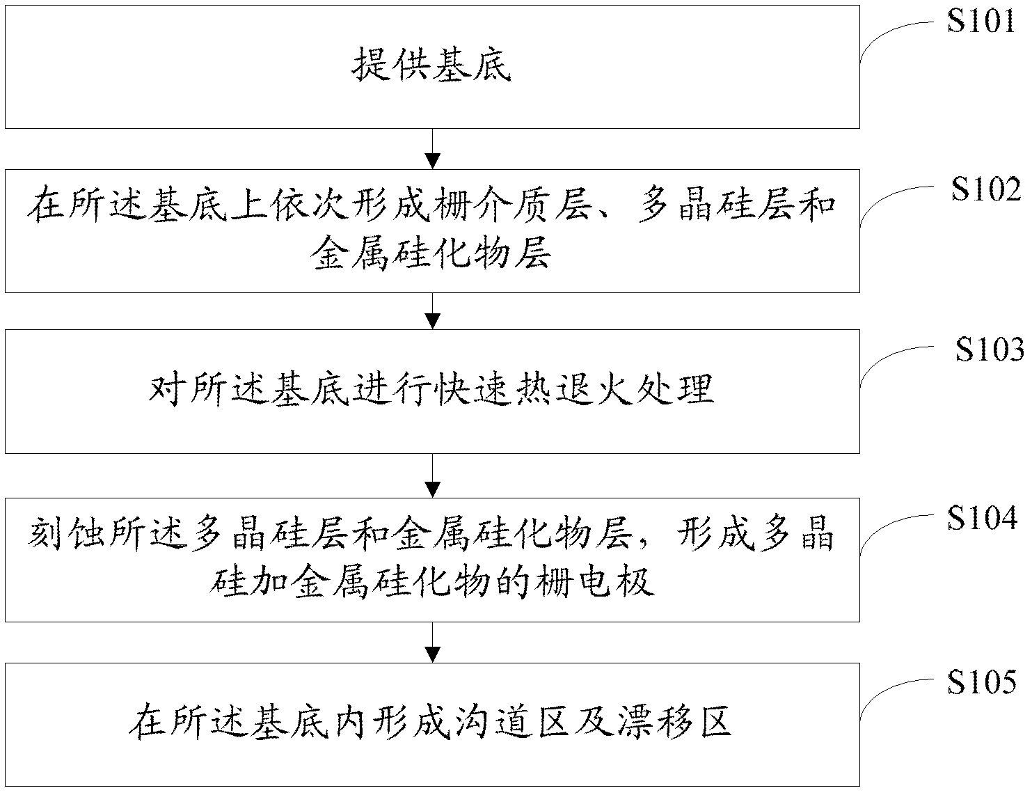
[0043] S101, providing a substrate.
[0044] refer to figure 2 , wherein the substrate 1 may be a silicon substrate. Of course, in other embodiments of the present invention, the substrate may also be a germanium substrate or a gallium arsenide substrate.
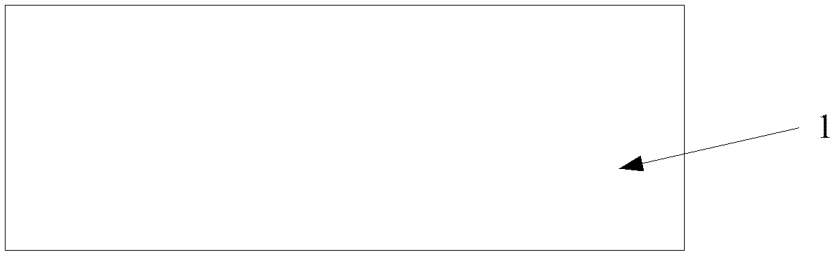
[0045] S102, sequentially forming a gate dielectric layer, a polysilicon layer, and a metal silicide layer on the substrate.
[0046] refer to image 3 , first forming a gate dielectric layer 2 on the substrate 1 . Wherein, the gate dielectric layer may be a silicon oxide layer. Those skilled in the art can understand that silicon oxide has a high dielectric strength (10 7 V / cm) and high resistivity (about 10 17 Ω·cm), so it is the preferred material for the gate dielectric layer. In practical applications, the thickness of the gate dielectric layer can be selected in a standa...
Embodiment 2
[0056] Such as Figure 7 As shown, another LDMOS device manufacturing method provided by the embodiment of the present invention includes:
[0057] S201, providing a substrate.
[0058] S202, sequentially forming a gate dielectric layer, a polysilicon layer and a metal silicide layer on the substrate.
[0059] S203, placing the substrate in a rapid heat treatment machine.
[0060] S204, heating the substrate in the rapid heat treatment machine to 1000°C.
[0061] S205, keeping the substrate in a rapid heat treatment machine for 1 min.
[0062] Of course, those skilled in the art can understand that other machines capable of performing rapid thermal annealing can also be used to perform rapid thermal annealing on the substrate. For devices with different technical requirements, the heating temperature and heating time for the rapid thermal annealing treatment of the substrate are different, which are not limited in the present invention.
[0063] S206 , etching the polysil...
Embodiment 3
[0066] Such as Figure 8 As shown, another LDMOS device manufacturing method provided by the embodiment of the present invention includes:
[0067] S301. Provide a substrate.
[0068] S302, sequentially forming a gate dielectric layer, a polysilicon layer and a metal silicide layer on the substrate.
[0069] S303, performing rapid thermal annealing treatment on the substrate.
[0070] S304. Spin-coat a photoresist layer on the metal silicide layer.
[0071] S305 , exposing the photoresist layer by means of a mask having a gate region pattern.
[0072] S306 , developing the exposed photoresist layer to form a photoresist layer with a gate region pattern.
[0073] S307 , using the photoresist layer with the gate region pattern as a mask to etch the polysilicon layer and the metal silicide layer to form a polysilicon plus metal silicide gate electrode.
[0074] S308, forming a channel region and a drift region in the substrate.
PUM
| Property | Measurement | Unit |
|---|---|---|
| Resistivity | aaaaa | aaaaa |
| Resistivity | aaaaa | aaaaa |
Abstract
Description
Claims
Application Information