Transverse parasitic plug-and-play (PNP) device in SiGe heterojunction bipolar transistor (HBT) technique and production method

A manufacturing method and process technology, which is applied in the field of semiconductor integrated circuits, can solve the problems of low triode early voltage, short emission region diffusion length, and poor device consistency, so as to reduce base diffusion current, improve performance, and increase amplification multiple effect

Active Publication Date: 2013-03-13
SHANGHAI HUAHONG GRACE SEMICON MFG CORP
View PDF5 Cites 4 Cited by
  • Summary
  • Abstract
  • Description
  • Claims
  • Application Information

AI Technical Summary

Problems solved by technology

[0002] The lateral parasitic PNP transistor in the conventional silicon germanium HBT process, its collector region is formed by high-dose, low-energy boron implantation plus an annealing impurity and/or traditional CMOS P-well implantation, so doped The impurity concentration is higher, and there is metal silicide on the emitter, which makes the diffusion length of the emitter region shorter, resultin

Method used


Image

  • Transverse parasitic plug-and-play (PNP) device in SiGe heterojunction bipolar transistor (HBT) technique and production method
  • Transverse parasitic plug-and-play (PNP) device in SiGe heterojunction bipolar transistor (HBT) technique and production method
  • Transverse parasitic plug-and-play (PNP) device in SiGe heterojunction bipolar transistor (HBT) technique and production method

Examples


Embodiment Construction

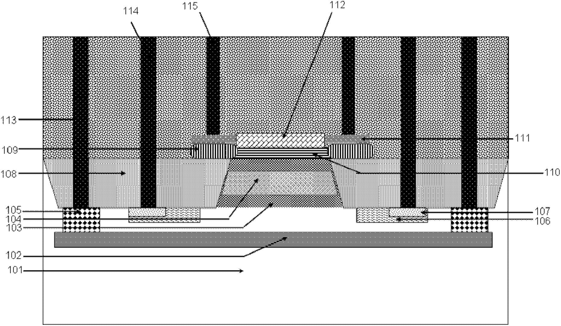
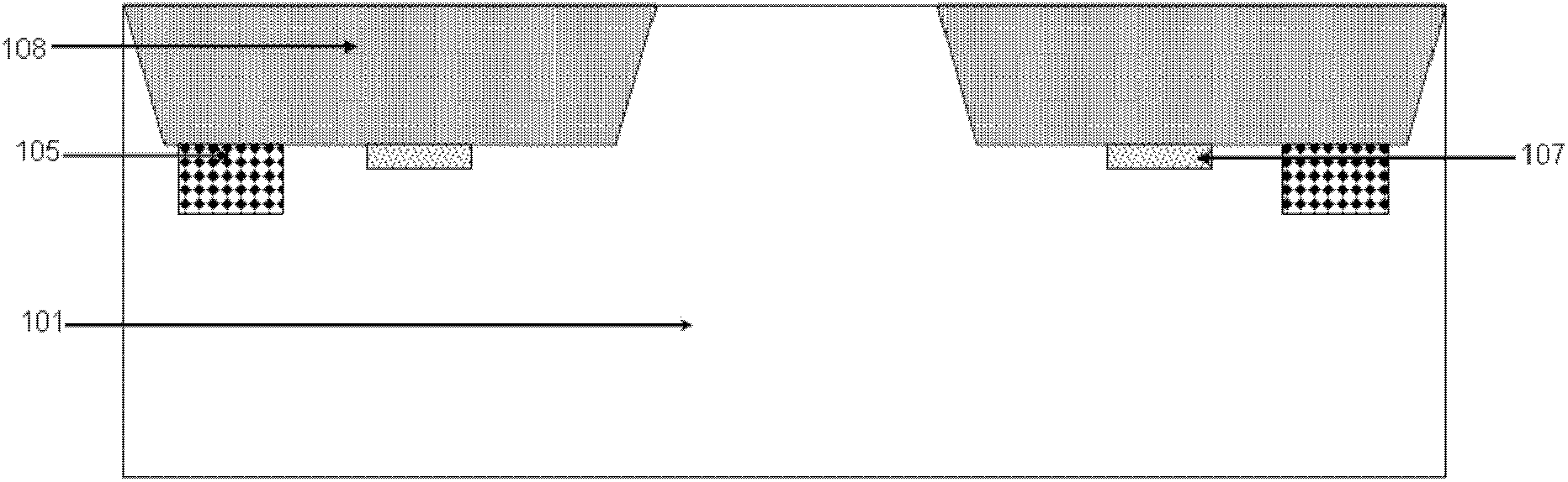
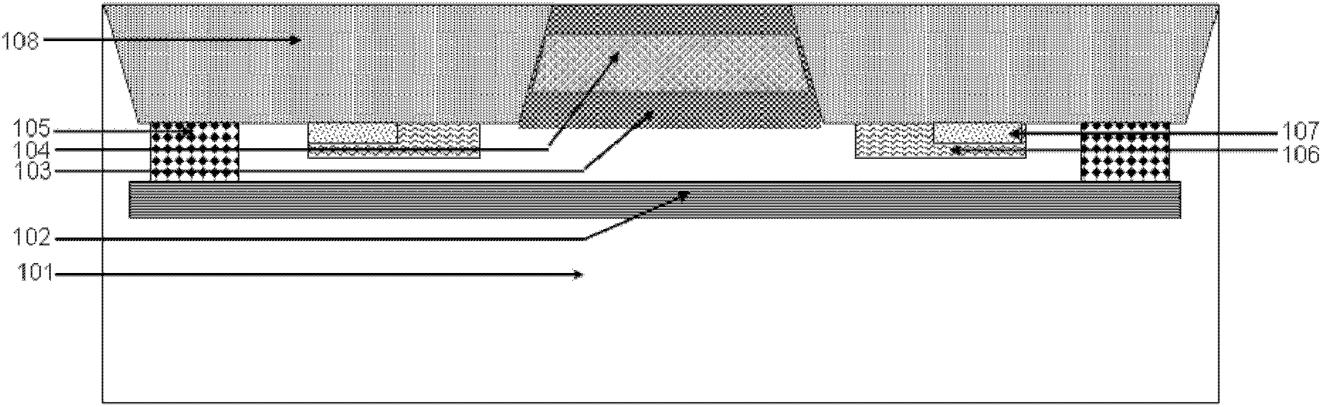
[0030] Such as figure 1 As shown, in the lateral parasitic PNP device in the silicon germanium HBT process of the embodiment of the present invention, the active region is composed of shallow trench field oxygen, i.e. figure 1 The shallow trench isolation layer 108 in isolation includes a collector region, a base region, an emitter region and an outer isolation region.

[0031] The collector region includes a P-type buried layer 107 formed at the bottom of the shallow trench on both sides of the active region, a P-type impurity ion implantation layer 106 formed at the bottom of the shallow trench and connected to the P-type buried layer 107, and the P-type buried The layer 107 is laterally separated from the base region by more than 1 micron, and the collector region is led out through a deep contact hole 114 in a corresponding shallow trench on top of the P-type buried layer 107 .

[0032] The base region is composed of an N-type impurity ion implantation layer formed on the...


PUM


Abstract

The invention discloses a transverse parasitic PNP device in the SiGe HBT technique. An active region is isolated by field oxide of a shallow groove; a collector region comprises P-type buried layers formed at the bottom of the shallow groove and on two sides of the active region and P-type impurity ion implanted layers formed at the bottom of the shallow groove and connected with the P-type buried layers, wherein the transverse distance between each P-type buried layer and a base region is larger than 1 micron; the base region is formed by an N-type impurity ion implanted layer formed on the upper portion of the active region; and an emitting region is formed by a P-type SiGe epitaxial layer formed on the N-type impurity ion implanted layer of the active region and a polysilicon layer formed at the top of the shallow groove and connected with the P-type SiGe epitaxial layer, wherein the upper portion of the P-type SiGe epitaxial layer is provided with a silicide barrier layer. The invention further discloses a production method of the PNP device. According to the device and the method, the performances of the PNP device are improved, SiGe free of metal silicide is formed in the emitting region, loss of silicon for the metal silicide is reduced, the thickness of the emitting region is increased, base diffusion current is reduced, and the DC amplification factor is increased.

Description

technical field [0001] The invention relates to the field of semiconductor integrated circuits, in particular to a lateral parasitic PNP device in a silicon-germanium HBT process. The invention also relates to a manufacturing method of the lateral parasitic PNP device in the silicon germanium HBT process. Background technique [0002] The lateral parasitic PNP transistor in the conventional silicon germanium HBT process, its collector region is formed by high-dose, low-energy boron implantation plus an annealing impurity and / or traditional CMOS P-well implantation, so doped The impurity concentration is higher, and the metal silicide on the emitter makes the diffusion length of the emitter region shorter, resulting in a larger diffusion current in the base region. In order to make the device have a proper DC current magnification, it is usually necessary to reduce the concentration and thickness of the base region to increase the diffusion current in the collector region, a...

Claims


Application Information

Patent Timeline
IPC IPC(8): H01L29/737H01L29/36H01L21/331H01L21/265
Inventor 周正良周克然
Owner SHANGHAI HUAHONG GRACE SEMICON MFG CORP
Why Eureka
Try Eureka