Green nitride light-emitting diode (LED) epitaxial wafer and growth method thereof

A technology of LED epitaxial wafers and growth methods, which is applied in the direction of electrical components, circuits, semiconductor devices, etc., can solve problems such as low hole injection efficiency, limited luminous efficiency, and mismatch between electron and hole concentrations, and achieve internal quantum efficiency. Reasonable process and the effect of improving internal quantum efficiency

Inactive Publication Date: 2013-03-13
YANGZHOU ZHONGKE SEMICON LIGHTING
View PDF3 Cites 18 Cited by
  • Summary
  • Abstract
  • Description
  • Claims
  • Application Information

AI Technical Summary

Problems solved by technology

The existence of the AlGaN barrier layer will further block the injection of holes into the quantum well to a certain extent, these factors will lead to low hole injection efficiency, so that the concentration of electrons and holes in the active region does not match seriously, Thereby limiting the luminous efficiency of LED

Method used


Image

  • Green nitride light-emitting diode (LED) epitaxial wafer and growth method thereof
  • Green nitride light-emitting diode (LED) epitaxial wafer and growth method thereof
  • Green nitride light-emitting diode (LED) epitaxial wafer and growth method thereof

Examples


Embodiment Construction

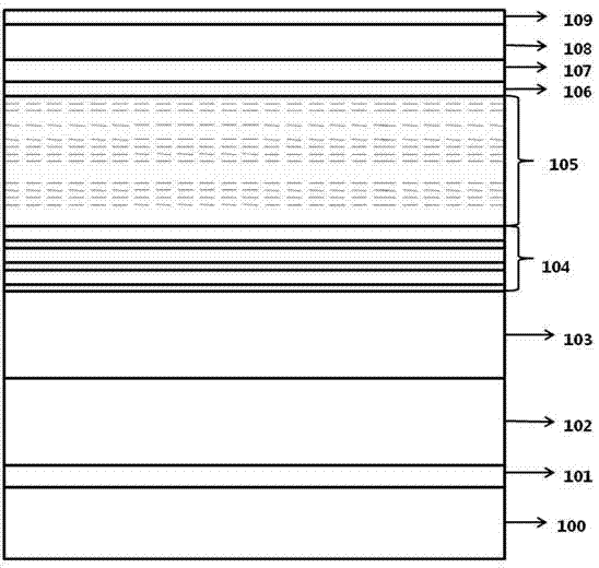
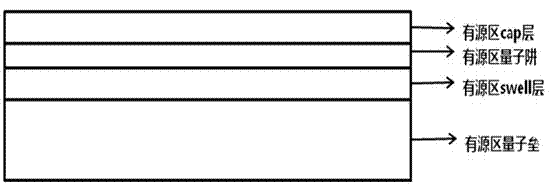
[0021] The present invention utilizes MOCVD equipment (G5 56 commercial machine of Aixtron Company), and used V group source is ammonia gas (NH 3 ), the Group III organic source materials are trimethylgallium (TMGa) and trimethylindium (TMIn), and the P-type and N-type doped well elements are respectively Mg and Si. The substrate can be any one of sapphire, silicon, silicon carbide or gallium arsenide. Such as figure 1 , 2 As shown, the specific steps of growth are as follows:

[0022] 1. Growing the low-temperature buffer layer 101 on the substrate 100: the growth temperature is 550° C., the pressure is 600 mbar, and the thickness of the formed low-temperature buffer layer 101 is 30 nm.

[0023] 2. Growing the unintentionally doped GaN layer 102 on the low-temperature buffer layer 101 : the growth temperature is 1100° C., the pressure is 600 mbar, and the thickness of the unintentionally doped GaN layer 102 is 1 μm.

[0024] 3. Growing the N-type electron injection layer ...


PUM


Abstract

The invention relates to a green nitride LED epitaxial wafer and a growth method thereof, and belongs to the technical field of semiconductor photo-electricity. The method is characterized in that an InGaN material layer with a low content of In components is grown between a quantum barrier and a quantum well in each quantum well active area when a plurality of quantum well active areas are grown; a quantum barrier is grown on a cap layer in a last quantum well active area, a hole injection layer is grown on the quantum well, and a p-AlGaN electronic blocking layer is grown on the hole injection layer. According to the green nitride LED epitaxial wafer and the growth method thereof, the process is reasonable, and the production is facilitated; LED chips are manufactured through a standard chip process, so that the internal quantum efficiency is improved, and the hole injection efficiency is improved greatly; and manufactured chips are high in luminous flux after being packaged, the inverse antistatic capacity reaches more than ten thousand volts, the electricity is not leaked under 8-volt inverse voltage measurement, and the working voltage is smaller than 3.1 volts under a 15 mA forward current.

Description

technical field [0001] The invention belongs to the technical field of semiconductor optoelectronics, in particular to the technical field of production of a nitride green LED epitaxial wafer. Background technique [0002] GaN-based blue-green light technology realizes the full coverage of LEDs in the visible light band. At the same time, because LED-based lighting technology has the characteristics of energy saving, environmental protection, non-toxic, non-polluting, fast response, solid light source, shock resistance, impact resistance, thinness and shortness, etc. , LED has now widely penetrated into our daily life, such as: signal indication and information display and other fields; liquid crystal display backlight, outdoor and indoor lighting fields; and radiation lighting functions in special fields such as biology and medical treatment. Among them, based on the flat panel display industry and the huge market in various lighting fields, LED planar light source has beco...

Claims


Application Information

Patent Timeline
Patent Type & Authority Applications(China)
IPC IPC(8): H01L33/06H01L33/14H01L33/00
Inventor 李盼盼李鸿渐李志聪李璟王国宏
Owner YANGZHOU ZHONGKE SEMICON LIGHTING
Why Eureka
Try Eureka