Large-dimension hexagonal bi-layer grapheme single-crystal domain and preparation method thereof

A double-layer graphene and hexagonal technology, applied in the field of nanomaterials, can solve the problems that affect the transportation properties of graphene, the number of layers cannot be adjusted, and it is limited to the range of hundreds of nanometers to tens of microns, and is suitable for large-scale Easy control of production and process, good quality effect

Active Publication Date: 2013-03-27
SHANGHAI INST OF CERAMIC CHEM & TECH CHINESE ACAD OF SCI
View PDF2 Cites 17 Cited by
  • Summary
  • Abstract
  • Description
  • Claims
  • Application Information

AI Technical Summary

Problems solved by technology

Therefore, during the transmission of electrons, a large amount of scattering will occur, which seriously affects the electrical transport properties of graphene.
Recently, researchers have tried to use atmos...

Method used


Image

  • Large-dimension hexagonal bi-layer grapheme single-crystal domain and preparation method thereof
  • Large-dimension hexagonal bi-layer grapheme single-crystal domain and preparation method thereof
  • Large-dimension hexagonal bi-layer grapheme single-crystal domain and preparation method thereof

Examples


Embodiment 1

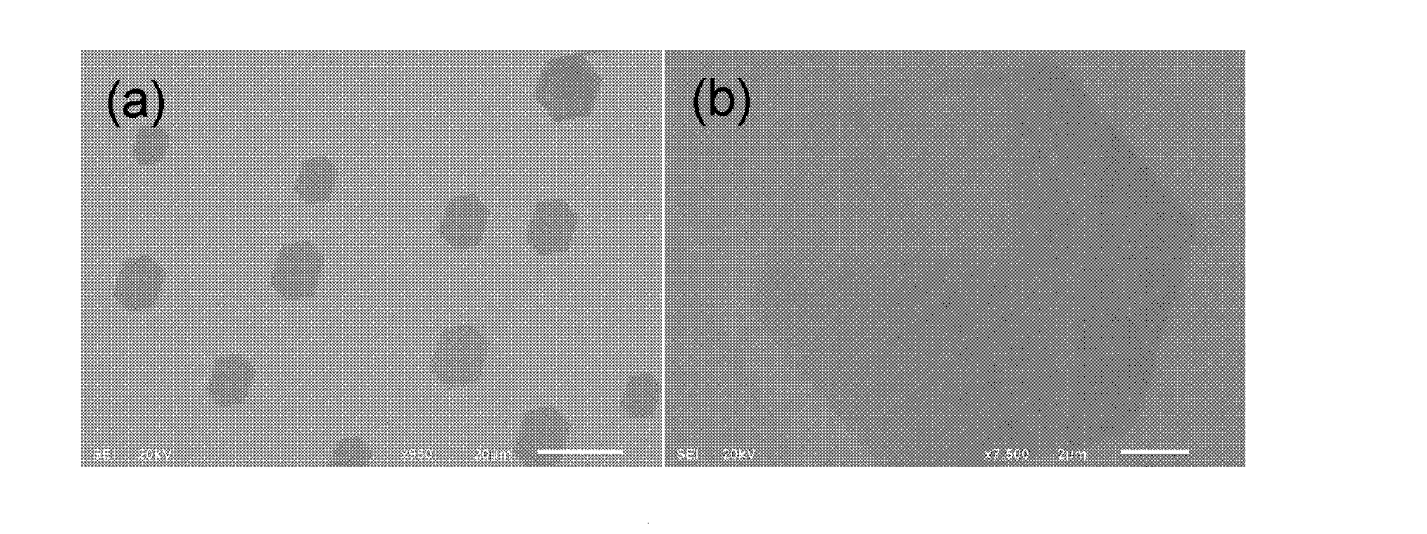
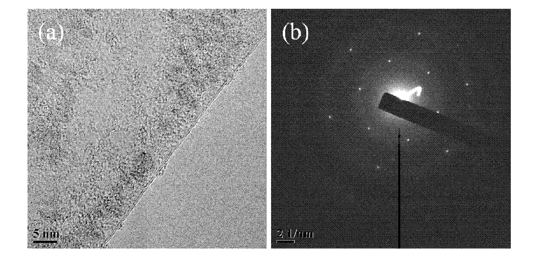
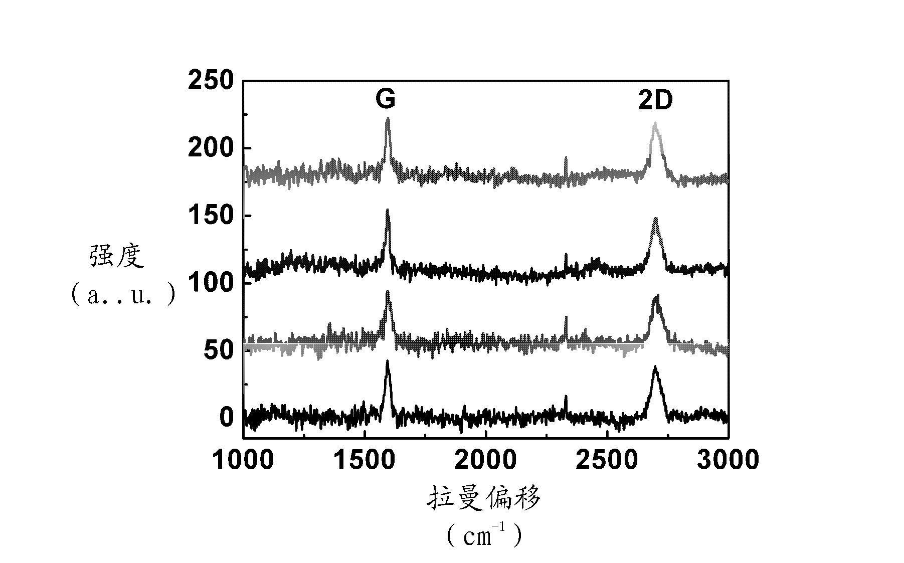
[0019] (1) Use 25 μm copper foil (purchased from Alfa (alfa) company, product number 13382) as a catalyst, put it into a chemical vapor deposition reaction furnace, feed 300 sccm hydrogen and 300 sccm argon, and start heating to 1000 ° C after 60 minutes, After constant temperature for 30 minutes, 20sccm methane, 200sccm hydrogen, 100sccm argon are introduced, and the reaction time is 20 minutes. After the reaction, stop passing methane, turn off the electric furnace, and rapidly cool to room temperature to obtain hexagonal graphene single crystal domains. Electron microscope photos such as figure 1 shown. Graphene is a double-layer structure, TEM photos and Raman spectra are as follows figure 2 The bilayer coverage shown is 93%.

Embodiment 2

[0021] The preparation method is basically the same as in Example 1, the difference being that a 600nm metal nickel film is deposited on a 25 μm Cu foil substrate by magnetron sputtering, and this binary alloy is used as a catalyst, and 200 sccm of hydrogen gas is introduced, and after 60 minutes Start heating to 1040°C, keep the temperature for 30 minutes, and then feed 2 sccm acetylene and 200 sccm hydrogen, and the reaction time is 60 minutes. Obtain graphene single crystal domains as bilayer structure ( figure 2 ), the graphene size is 40–80 μm, and the bilayer coverage is 95%.

Embodiment 3

[0023] The preparation method is basically the same as in Example 1, the difference is: adopt copper-nickel alloy (Cu0.7Ni0.3) as the catalyst, feed 800 sccm hydrogen, start heating to 1040 ° C after 60 minutes, and feed 10 sccm nitrogen drum after 30 minutes at constant temperature Soak ethanol, 400s ccm hydrogen, and the reaction time is 5 hours. The obtained graphene single crystal domain is a bilayer structure, the graphene size is 100 μm, and the bilayer coverage is 92%.


PUM

PropertyMeasurementUnit
Sizeaaaaaaaaaa
Sizeaaaaaaaaaa

Abstract

The invention belongs to the field of nano-materials, and relates to a novel large-dimension hexagonal bi-layer grapheme single-crystal domain and a preparation method thereof. The preparation method comprises the steps that: elemental metal and a multi-element alloy thereof are adopted as a catalyst; and the hexagonal grapheme single-crystal domain is prepared with a chemical vapor deposition method. The grapheme single-crystal domain has a bi-layer structure, excellent quality, and bi-layer coverage higher than 90%. The method provided by the invention has the advantages of simple process and easy-to-control procedure. The large-dimension hexagonal bi-layer grapheme single-crystal domain and the preparation method thereof are suitable for the field of micro-nano-electronic and photonic devices such as transistor, light modulator, and the like.

Description

technical field [0001] The invention belongs to the field of nanomaterials, and relates to a large-scale double-layer graphene single crystal domain, a preparation method thereof, and the application of the large-scale double-layer graphene single crystal domain in the field of micro-nano electronics and photonic devices. Background technique [0002] Graphene is a two-dimensional (2D) periodic honeycomb lattice structure composed of carbon six-membered rings. The unique crystal structure of graphene gives it excellent properties, such as high thermal conductivity, high mechanical strength, and unique electrical and optical properties. . Graphene is essentially a semi-metal, but in order to be applied in the semiconductor industry, the regulation of the band gap is necessary. Recently, a continuously tunable band structure can be obtained with bilayer graphene, which is very important for electronic and optoelectronic device applications. At present, the best bilayer graph...

Claims


Application Information

Patent Timeline
IPC IPC(8): C30B29/02C30B29/60C30B29/68C30B25/00C01B31/06C01B32/186
Inventor 黄富强毕辉万冬云林天全
Owner SHANGHAI INST OF CERAMIC CHEM & TECH CHINESE ACAD OF SCI
Why Eureka
Try Eureka