Formation method of groove-shaped semiconductor structure

A semiconductor and trench technology, used in semiconductor/solid-state device manufacturing, electrical components, circuits, etc., can solve the problems of poor process uniformity, easy generation of large pressure, deformation of silicon wafers, etc., to achieve low defect density, reduce Stress, Defect Prevention Effect

Inactive Publication Date: 2013-04-10
SHANGHAI HUAHONG GRACE SEMICON MFG CORP
View PDF7 Cites 7 Cited by
  • Summary
  • Abstract
  • Description
  • Claims
  • Application Information

AI Technical Summary

Problems solved by technology

Polycrystalline or amorphous silicon trenches are generally placed in single crystal silicon. Due to the difference in crystal structure, the thermal expansion coefficients of polycrystalline or amorphous silicon and single crystal silicon are quite different. The thermal expansion coefficient of single crystal silicon is about 3.0 , while the thermal expansion coefficient of polycrystalline or amorphous silicon is around 6.0, so devices with polycrystalline or amorphous silicon trench structures tend to generate greater pressure after undergoing subsequent thermal processes, especially for relatively high ...

Method used


Image

  • Formation method of groove-shaped semiconductor structure
  • Formation method of groove-shaped semiconductor structure
  • Formation method of groove-shaped semiconductor structure

Examples


Embodiment 1

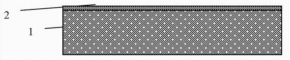
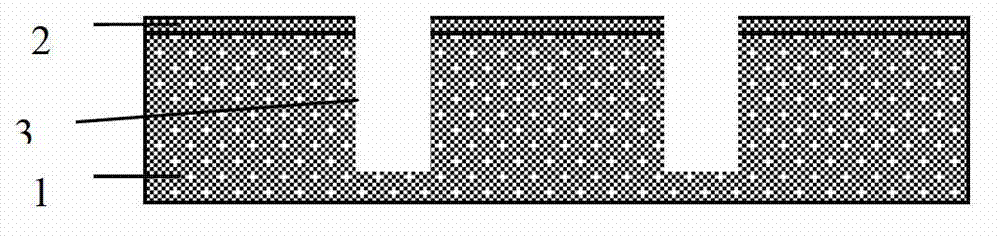
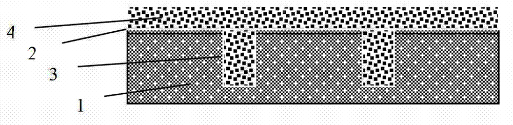
[0032] likeFigure 1A-Figure 1D As shown, the manufacturing process of this embodiment 1 includes the following steps:

[0033] 1) Dielectric layer growth. Dielectric film 2 is grown on silicon substrate or silicon epitaxy 1, and dielectric film 2 is SiO 2 , SiN, SiON at least one (see Figure 1A ), the growth of the dielectric film 2 can be grown by chemical vapor deposition or thermal oxidation, the growth temperature is 300-1300 degrees Celsius, and the growth pressure is 0.01-760 Torr; the thickness of the dielectric film 2 is 0.1-5.0 microns.

[0034] 2) Trench etching. Groove etching adopts anisotropic dry etching, and uses photoresist as a mask to etch a groove 3 in a predetermined area. The width of the groove 3 is 0.1-5.0 microns, and the depth of the groove 3 is 0.1 -10 µm (see Figure 1B ).

[0035] 3) C-containing polysilicon or amorphous silicon 4 filling. Fill the entire trench 3 with C-doped polysilicon or amorphous silicon (i.e. C-containing polysilicon or...

Embodiment 2

[0039] like Figure 2A-Figure 2D Shown, the manufacturing process of embodiment 2 comprises the following steps:

[0040] 1) Dielectric layer growth. Dielectric film 2 is grown on silicon substrate or silicon epitaxy 1, and dielectric film 2 is SiO 2 , SiN, SiON at least one (see Figure 2A ), the growth of the dielectric film 2 can be grown by chemical vapor deposition or thermal oxidation, the growth temperature is 300-1300 degrees Celsius, and the growth pressure is 0.01-760 Torr; the thickness of the dielectric film 2 is 0.1-5.0 microns.

[0041] 2) Trench etching. Groove etching adopts anisotropic dry etching, and uses photoresist as a mask to etch a groove 3 in a predetermined area. The width of the groove 3 is 0.1-5.0 microns, and the depth of the groove 3 is 0.1 -10 µm (see Figure 2B ).

[0042] 3) Polycrystalline SiC or amorphous SiC filling. Fill the entire trench 3 with SiC-doped polycrystalline SiC or amorphous SiC 5 (see Figure 2C ). Polycrystalline SiC...

Embodiment 3

[0046] like Figure 3A-Figure 3D Shown, the manufacturing process of embodiment 3 comprises the following steps:

[0047] 1) Trench etching. Groove etching adopts anisotropic dry etching, and uses photoresist as a mask to etch a groove 3 in a predetermined area on the silicon substrate or silicon epitaxy 1, and the width of the groove 3 is 0.1-5.0 microns , the depth of groove 3 is 0.1-10 microns (see Figure 3A ).

[0048] 2) Thermal oxide film growth on all silicon wafers. At a temperature of 700-1300 degrees Celsius, in O 2 , or H 2 O and O 2 Under the atmosphere, thermally oxidize the sidewall and top of trench 3 to form silicon oxide 6 of 0.01-0.5 microns (see Figure 3B ).

[0049] 3) C-containing polysilicon or amorphous silicon filling. Fill the entire trench with C-doped polysilicon or amorphous silicon (i.e. C-containing polysilicon or amorphous silicon4) (see Figure 3C ). C-containing polysilicon or amorphous silicon 4 adopts the method of chemical vapor...


PUM

PropertyMeasurementUnit
Thicknessaaaaaaaaaa
Thicknessaaaaaaaaaa

Abstract

The invention discloses a formation method of a groove-shaped semiconductor structure. Due to the fact that polycrystalline silicon or amorphous silicon is mixed with carbide (C) to fill a groove, or polycrystalline silicon carbide (Si C) or amorphous Si C replaces the polycrystalline silicon or the amorphous silicon to fill the groove, stress of a component is capable of being reduced, and thereby defects inside silicon caused by the stress of the polycrystalline silicon or the amorphous silicon are prevented, and therefore the trench gate semiconductor structure with low stress and defect concentration or a groove access with low resistance is obtained.

Description

technical field [0001] The invention belongs to a semiconductor process method in a semiconductor integrated circuit, in particular to a method for forming a trench-shaped semiconductor structure. Background technique [0002] Polycrystalline or amorphous silicon trench structures are widely used in various semiconductor devices, such as trench MOSFET (Metal-Oxide-Semiconductor Field-Effect Transistor, gold oxide half field effect transistor) and IGBT (Insulated Gate Bipolar Transistor, insulation gate bipolar transistors), low-resistance vertical conduction paths in radio frequency semiconductor devices, etc. Polycrystalline or amorphous silicon trenches are generally placed in single crystal silicon. Due to the difference in crystal structure, the thermal expansion coefficients of polycrystalline or amorphous silicon and single crystal silicon are quite different, and the thermal expansion coefficient of single crystal silicon is around 3.0. , while the thermal expansion ...

Claims


Application Information

Patent Timeline
IPC IPC(8): H01L21/02
Inventor 刘继全
Owner SHANGHAI HUAHONG GRACE SEMICON MFG CORP
Why Eureka
Try Eureka