Eureka AIR delivers breakthrough ideas for toughest innovation challenges, trusted by R&D personnel around the world.

Metal aluminum base aluminum nitride package substrate and preparation method thereof

A technology based on aluminum nitride sealing and packaging substrates, which is applied in the field of microelectronic materials to achieve the effect of improving thermal shock resistance

Inactive Publication Date: 2013-04-10
WUHAN BOOYEN TECH
View PDF7 Cites 7 Cited by
  • Summary
  • Abstract
  • Description
  • Claims
  • Application Information

AI Technical Summary

Problems solved by technology

A buffer layer is used between the metal and the aluminum nitride film, such as Cr, Ni, Ti and other metals. The buffer layer is generally tens to hundreds of nanometers, which helps to improve the bonding strength of the aluminum nitride film and the metal substrate, and can be certain To some extent, the difference in thermal expansion coefficient between the aluminum nitride film and the metal substrate can be alleviated, but it cannot completely solve the problem

Method used


Image

  • Metal aluminum base aluminum nitride package substrate and preparation method thereof
  • Metal aluminum base aluminum nitride package substrate and preparation method thereof

Examples


Embodiment 1

[0026] 1. Use a tablet press to flatten the aluminum sheet with a thickness of 2mm under a pressure of 10MPa.

[0027] 2. Anneal at a temperature of 500°C for 3 hours to eliminate the internal stress of the aluminum sheet.

[0028] 3. Routine dewaxing, degreasing, pickling, alkali washing, deionized water cleaning.

[0029] 4. Electrochemical polishing: perform electrochemical polishing in the polishing solution of perchloric acid and absolute ethanol 1:4 for 2 minutes, and the current density is 10A / dm 2 .

[0030] 5. Anodic oxidation: The electrolyte is 0.3mol / L oxalic acid, and the anodic oxidation temperature and anodic oxidation voltage are adjusted by gradient:

[0031] The first level: temperature -30 ℃, voltage 200V, time 10 minutes;

[0032] Second stage: temperature -15°C, voltage 100V, time 10 minutes;

[0033] The third stage: the temperature is 4°C, the voltage is 40V, the time is 20 minutes, and the anodic oxidation is completed. The anodized aluminum film i...

Embodiment 2

[0038] 1. Use a tablet press to flatten the aluminum sheet with a thickness of 2mm under a pressure of 10MPa.

[0039] 2. Anneal at a temperature of 500°C for 3 hours to eliminate the internal stress of the aluminum sheet.

[0040] 3. Routine dewaxing, degreasing, pickling, alkali washing, deionized water cleaning.

[0041]4. Electrochemical polishing: perform electrochemical polishing in the polishing solution of perchloric acid and absolute ethanol 1:4 for 2 minutes, and the current density is 10A / dm 2 .

[0042] 5. Anodic oxidation: The electrolyte is 0.3mol / L oxalic acid, and the anodic oxidation temperature and anodic oxidation voltage are adjusted by gradient:

[0043] The first level: temperature -30 ℃, voltage 200V, time 30 minutes;

[0044] Second stage: temperature -15°C, voltage 100V, time 60 minutes;

[0045] The third stage: the temperature is 4°C, the voltage is 40V, the time is 120 minutes, and the anodic oxidation is completed. The anodized aluminum film i...

Embodiment 3

[0050] 1. Use a tablet press to flatten the aluminum sheet with a thickness of 2mm under a pressure of 10MPa.

[0051] 2. Anneal at a temperature of 500°C for 3 hours to eliminate the internal stress of the aluminum sheet.

[0052] 3. Routine dewaxing, degreasing, pickling, alkali washing, deionized water cleaning.

[0053] 4. Electrochemical polishing: perform electrochemical polishing in the polishing solution of perchloric acid and absolute ethanol 1:4 for 2 minutes, and the current density is 10A / dm 2 .

[0054] 5. Anodic oxidation: The electrolyte is 0.3mol / L oxalic acid, and the anodic oxidation temperature and anodic oxidation voltage are adjusted by gradient:

[0055] The first level: temperature -30 ℃, voltage 200V, time 10 minutes;

[0056] Second stage: temperature -15°C, voltage 100V, time 20 minutes;

[0057] The third stage: the temperature is 4°C, the voltage is 40V, the time is 40 minutes, and the anodic oxidation is completed. The anodized aluminum oxide ...


PUM

PropertyMeasurementUnit
thicknessaaaaaaaaaa
thicknessaaaaaaaaaa
strengthaaaaaaaaaa

Abstract

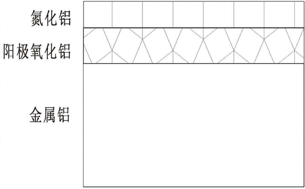
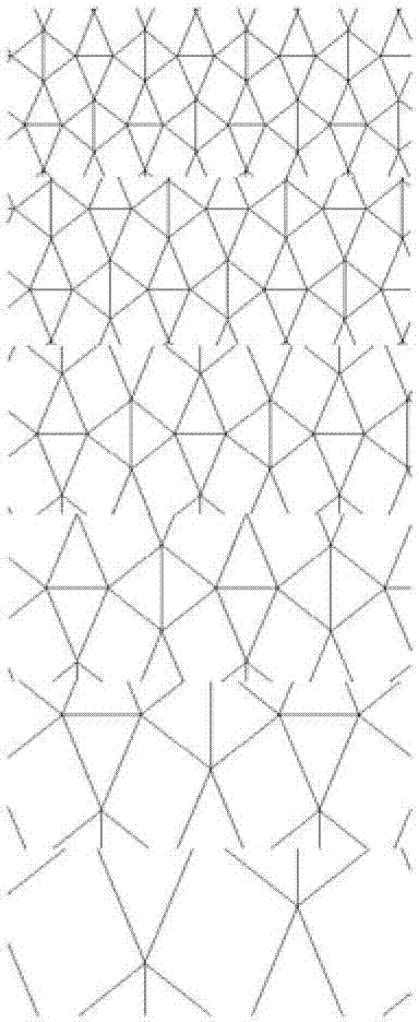
The invention discloses a metal aluminum base aluminum nitride package substrate and a preparation method thereof, and belongs to the field of microelectronic materials. The package substrate comprises a metal aluminum base, a porous anodic alumina film formed on the surface of the metal aluminum base, and an aluminum nitride film formed on the surface of the anodic alumina film, wherein the porosity of the anodic alumina film is reduced gradually along the direction from the metal aluminum base to the aluminum nitride film. According to the preparation method of the package substrate, metal aluminum is used as the base, anodic oxidation is carried out on one surface of aluminum to generate a layer of the porous anodic alumina film, and then the aluminum nitride film is deposited on the anodic alumina film in a vacuum mode. According to the metal aluminum base aluminum nitride package substrate, the anodic oxidation is carried out on the metal aluminum base, an anodic alumina thermal stress buffer layer with a coefficient of thermal expansion gradually varied is formed between the aluminum base and the aluminum nitride film, thermal shock resistance is improved obviously, cracking does not occur under 300 DEG C thermal shock, and therefore the metal aluminum base aluminum nitride package substrate can be applied in a subsequent process of semiconductor chip package well.

Description

technical field [0001] The invention relates to the technical field of microelectronic materials, and is mainly used in the packaging of high-power semiconductor chips, especially a metal aluminum-based aluminum nitride packaging substrate with high insulation, high thermal conductivity, and high thermal shock resistance and a preparation method thereof . Background technique [0002] With the vigorous development of semiconductor lighting and power semiconductor electronics, the application of high-power semiconductor chips is becoming more and more extensive. For the packaging of high-power semiconductor chips, the packaging substrate first needs to have high electrical strength to achieve electrical insulation, and at the same time needs to have high thermal conductivity so that the heat of the chip product can be conducted out in time. If the heat dissipation performance is not good, the life of the chip will be greatly shortened. [0003] Materials with high thermal c...

Claims


Application Information

Patent Timeline
Patent Type & Authority Applications(China)
IPC IPC(8): H01L23/14H01L23/373H01L21/48C23C28/02C25D11/02
Inventor 王文峰张军李明鹤彭雷
Owner WUHAN BOOYEN TECH
Why Eureka
Eureka Blog
Learn More