

Method for preparing monocrystal Bi2Se3 nano structure
A nanostructure, single crystal technology, applied in the direction of single crystal growth, nanotechnology, single crystal growth, etc., can solve the problems that are not conducive to the research of spintronics and quantum computer devices, affect the purity of materials, change and other problems, and achieve the production cost. Inexpensive, reproducible results
- Summary
- Abstract
- Description
- Claims
- Application Information
AI Technical Summary
Problems solved by technology
Method used
Image

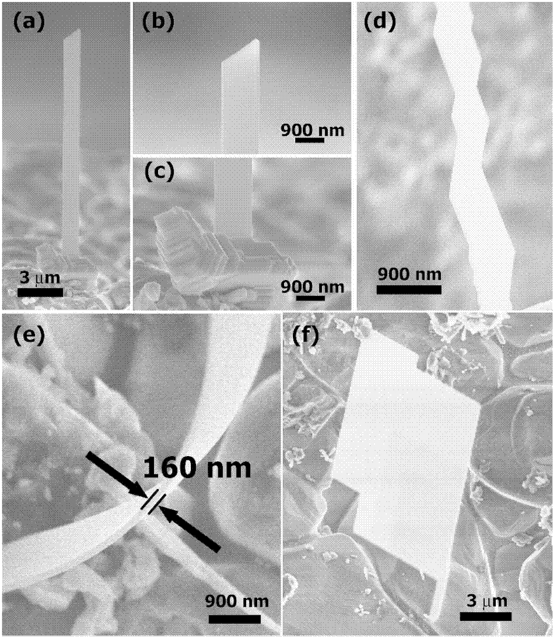
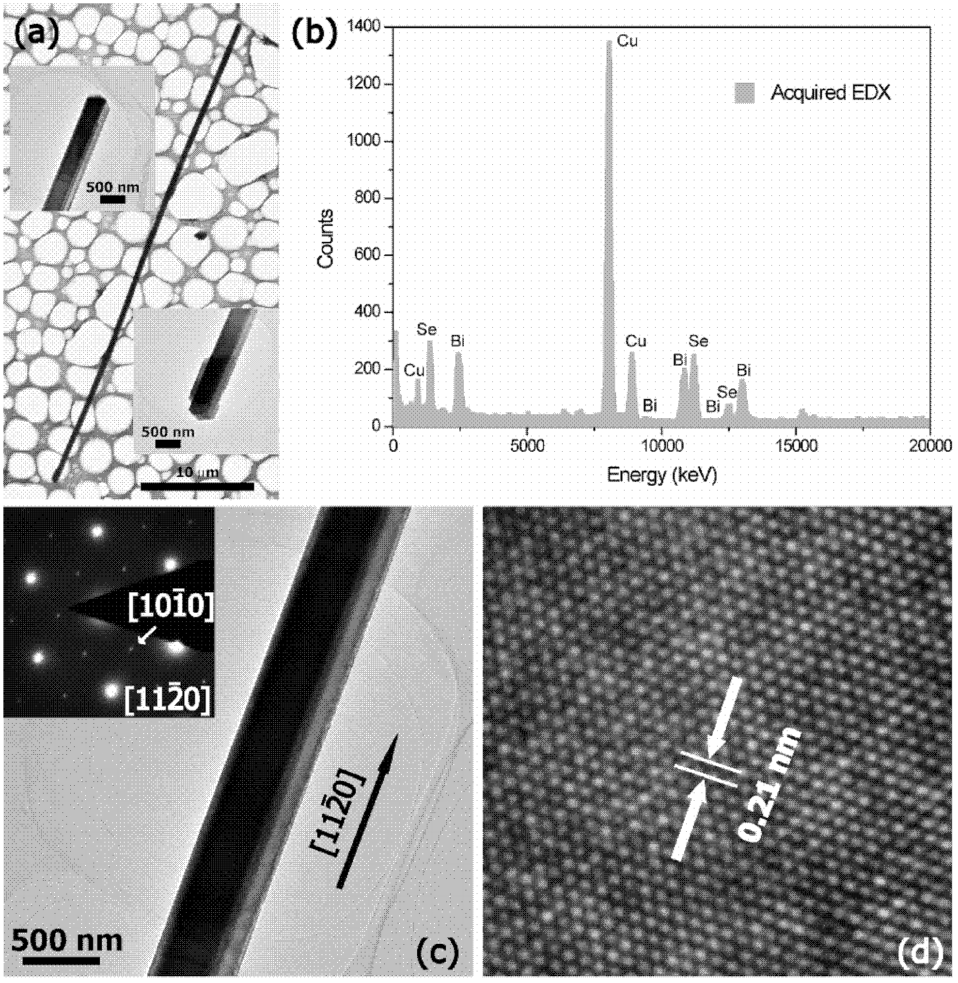
Examples
Embodiment 1
[0032] The first step, the Bi powder (purity 99.99% (weight ratio), Alfa Aesa) and Se powder (purity 99.99% (weight ratio), Alfa Aesa) that the mol ratio is 2: 3 mix homogeneously, put into quartz boat (up to Antu Technology) as a growth source;
[0033] In the second step, place the quartz boat in the middle of the horizontal tubular growth furnace (Tianjin Zhonghuan Experimental Electric Furnace Co., Ltd., model SK2-4-13), and place it at a distance of 5-15 cm from the quartz boat in the horizontal tubular growth furnace and away from the progressing furnace. A single crystal silicon wafer is placed at one end of the gas port as a substrate to collect the product;
[0034] The third step is to seal the horizontal tubular growth furnace and evacuate it so that the pressure of the horizontal tubular growth furnace reaches 1Pa;
[0035] The fourth step is to feed argon gas (purity 99.99% (weight ratio)) into the horizontal tube growth furnace at a flow rate of 50 sccm, so that...
Embodiment 2
[0039] The first step, the Bi powder (purity 99.99% (weight ratio), Alfa Aesa) and Se powder (purity 99.99% (weight ratio), Alfa Aesa) that the mol ratio is 2: 20 mix homogeneously, put on the quartz boat as source of growth;
[0040] In the second step, the quartz boat is placed in the middle of the horizontal tube growth furnace, and an alumina ceramic sheet is placed as a substrate at the end of the horizontal tube growth furnace 5-15 cm away from the quartz boat and away from the air inlet to collect the generated thing;
[0041] The third step is to seal the horizontal tubular growth furnace and evacuate it so that the pressure of the horizontal tubular growth furnace reaches 1Pa;
[0042] The fourth step is to feed argon gas into the horizontal tube growth furnace at a flow rate of 100 sccm so that the pressure of the horizontal tube growth furnace reaches 800 Pa;
[0043] The fifth step is to heat the horizontal tube growth furnace to 500°C and maintain the temperatur...
Embodiment 3
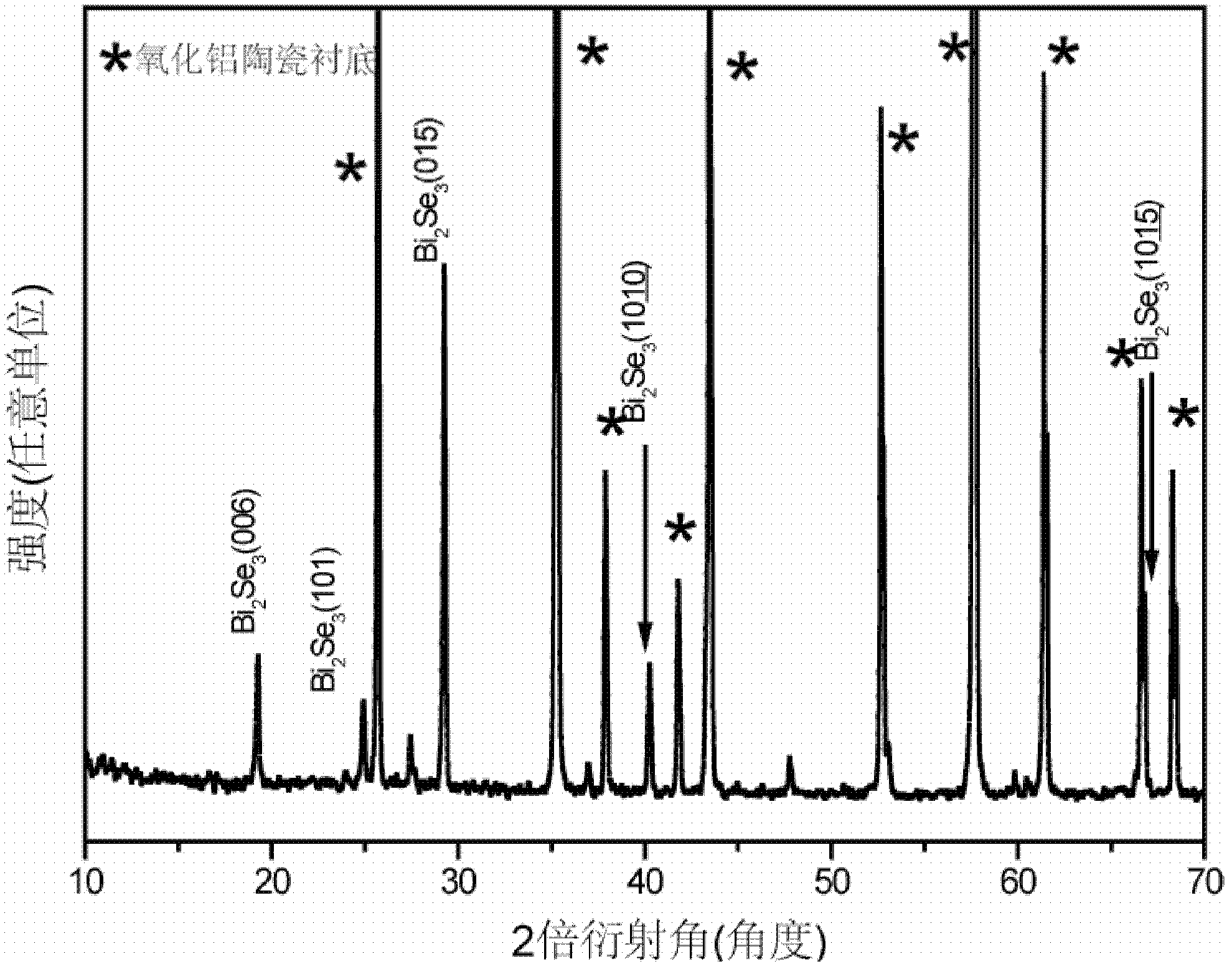
[0046] In the first step, Bi 2 Se 3 Powder (purity 99.999% (weight ratio), Sichuan Xinlong Tellurium Technology Co., Ltd.) is put on the quartz boat as a growth source;
[0047] In the second step, the quartz boat is placed in the middle of the horizontal tube growth furnace, and the alumina ceramic sheet is placed at the end of the horizontal tube growth furnace at a distance of 5 to 15 cm from the quartz boat and away from the air inlet. Growth of SiO on monocrystalline silicon wafers 2 The resulting silicon wafer is used as a substrate to collect the product;
[0048] The third step is to seal the horizontal tube growth furnace and evacuate it so that the pressure of the horizontal tube growth furnace reaches the lowest value that the vacuum equipment can provide;
[0049] The fourth step is to feed nitrogen gas (purity 99.99% (weight ratio)) into the horizontal tubular growth furnace at a flow rate of 50 sccm, so that the pressure of the horizontal tubular growth furnac...
PUM
 Abstract
Description
Claims
Application Information