Material structure for improving ohmic contact of p-GaN film and preparation method thereof

A technology of material structure and ohmic contact, which is applied in the direction of electrical components, circuits, semiconductor devices, etc., can solve the problem that p-GaN thin films cannot simply achieve low contact resistance, the hole concentration of p-GaN cannot be further increased, and the use of p -GaN film and other problems, to achieve the effect of improving ohmic contact performance, reducing specific contact resistivity, and good repeatability

Inactive Publication Date: 2013-05-01
INST OF SEMICONDUCTORS - CHINESE ACAD OF SCI
View PDF6 Cites 9 Cited by
  • Summary
  • Abstract
  • Description
  • Claims
  • Application Information

AI Technical Summary

Problems solved by technology

[0005] Due to the large forbidden band width of the P-GaN film, no metal work function can meet the requirements of forming an ohmic contact with it, and the hole concentration of p-GaN cannot be further increased (the maximum is about 1×10 18 cm -3 ), which leads to the fact that the ohmic contact of p-GaN film cannot simply achieve low contact resistance

Method used


Image

  • Material structure for improving ohmic contact of p-GaN film and preparation method thereof
  • Material structure for improving ohmic contact of p-GaN film and preparation method thereof
  • Material structure for improving ohmic contact of p-GaN film and preparation method thereof

Examples


Embodiment Construction

[0020] In order to make the object, technical solution and advantages of the present invention clearer, the present invention will be described in further detail below in conjunction with specific embodiments and with reference to the accompanying drawings.

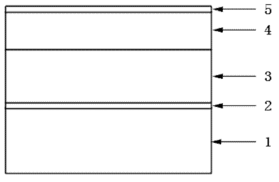
[0021] Such as figure 1 as shown, figure 1 It is a schematic diagram of the material structure of the improved p-GaN thin film ohmic contact provided by the present invention, and the material structure includes: a substrate 1; a buffer layer 2 grown on the substrate 1; n-GaN grown on the buffer layer 2 thin film layer 3; a p-GaN thin film layer 4 grown on the n-GaN thin film layer 3; and a heavily doped p-GaN thin film layer (p ++ - GaN thin film layer) 5.

[0022] Among them, the substrate 1 is made of sapphire, silicon, silicon carbide, gallium nitride or gallium arsenide, the buffer layer 2 is a GaN or AlN buffer layer grown at a low temperature around 500°C, and the n-GaN thin film layer 3 is GaN doped with Si impu...


PUM

PropertyMeasurementUnit
Thicknessaaaaaaaaaa
Growth temperatureaaaaaaaaaa
Thicknessaaaaaaaaaa

Abstract

The invention discloses a material structure for improving the ohmic contact of a p-GaN film and a preparation method thereof, wherein the material structure comprises a substrate (1), a buffer layer (2), an n-GaN film layer (3), a p-GaN film layer (4) and a heavily-doped p-GaN film layer (5), wherein the buffer layer (2) grows on the substrate (1); the n-GaN film layer (3) grows on the buffer layer (2); the p-GaN film layer (4) grows on the n-GaN film layer (3); and the heavily-doped p-GaN film layer (5) grows on the p-GaN film layer (4). According to the invention, the thin heavily-doped p-GaN layer with a large number of defects is inserted between the p-GaN film and a metal, and the heavily-doped p-GaN layer is enabled to have a large number of defect-energy levels by the methods of low-temperature growth or ion injection and the like, so that the transportation of current carriers can be finished through variable-range hopping or defect-energy level assistance, and furthermore, the specific contact resistivity of the p-GaN film and the contacted metal can be decreased, and the ohmic-contact performance of the p-GaN film is improved.

Description

technical field [0001] The invention relates to the technical field of semiconductors, in particular to a material structure for improving the ohmic contact of a p-GaN thin film and a preparation method thereof. Background technique [0002] Gallium nitride (GaN) is a third-generation semiconductor material with a wide band gap. It is a series of materials composed of indium and aluminum (including aluminum nitride, aluminum gallium nitride, indium gallium nitride, indium nitride, aluminum indium gallium nitride ) is widely used in light-emitting diodes (LEDs), blue lasers (Blue Lasers), solar cells and ultraviolet detection due to its large band gap, wide spectral range (covering the entire range from ultraviolet to infrared), high temperature resistance and corrosion resistance. It has important application value in the fields of optoelectronics and microelectronics such as devices. [0003] At present, people can use molecular beam epitaxy (MBE) and metal organic chemica...

Claims


Application Information

Patent Timeline
IPC IPC(8): H01L29/45H01L21/28
Inventor 吴亮亮赵德刚江德生刘宗顺陈平李亮乐伶聪杨辉
Owner INST OF SEMICONDUCTORS - CHINESE ACAD OF SCI
Why Eureka
Try Eureka