Multilayer film structure for improving conversion efficiency of crystalline silicon solar cell
A solar cell and conversion efficiency technology, applied in the direction of circuits, electrical components, semiconductor devices, etc., can solve problems such as inappropriate passivation of solar cells, and achieve the effect of excellent film uniformity and high deposition rate
- Summary
- Abstract
- Description
- Claims
- Application Information
AI Technical Summary
Problems solved by technology
Method used
Image

Examples
Embodiment 1
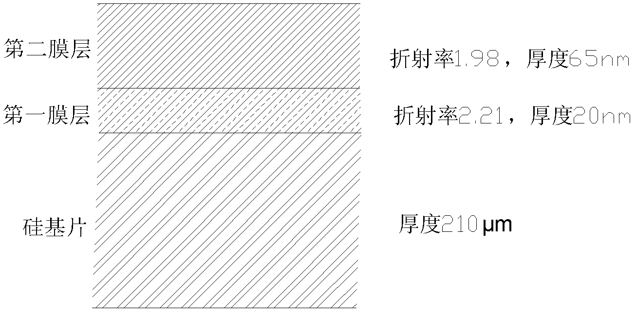
[0027] Forming a multilayer film structure to improve crystalline silicon solar cells Using microwave PECVD, a mixed gas of silane, ammonia and nitrogen is passed to deposit the first film layer on the cell substrate, and then the gas mixture is passed to deposit the second film on the first film layer layer; during the deposition process, the pressure is 40Pa; the gas flow rate is 440sccm for silane, 1850sccm for ammonia and 500sccm for nitrogen; and the microwave power density is 3000W.
Embodiment 2
[0029] Additionally, nitrogen will be removed from the conventional precursor gas so that the precursor gas includes silane and ammonia as source gases. The hydrogen concentration of the deposited SiN layer can have suitable film properties for passivation / anti-reflection.
[0030] Also, the mass density of SiN affects the hydrogen concentration during the sintering process. After sintering, for very low density SiN eg 2.2g / g / cm 3 , the hydrogen concentration can be reduced by 60%, and for higher density SiN layers, the hydrogen loss is negligible. It can be assured that the annealed layer has a mass density loss of less than 2.6 g / cm 3 , can allow excess hydrogen atoms to move during the sintering process, so that hydrogen molecules form and diffuse out of the SiN layer. Conversely, it is believed that having a higher than 2.8g / cm 3 With a mass density of , it does not allow sufficient hydrogen mobility during the sintering process, thus avoiding the migration of hydrogen...
PUM
| Property | Measurement | Unit |
|---|---|---|
| Thickness | aaaaa | aaaaa |
| Thickness | aaaaa | aaaaa |
Abstract
Description
Claims
Application Information
 - R&D
- Intellectual Property
- Life Sciences
- Materials
- Tech Scout
- Unparalleled Data Quality
- Higher Quality Content
- 60% Fewer Hallucinations
Browse by: Latest US Patents, China's latest patents, Technical Efficacy Thesaurus, Application Domain, Technology Topic, Popular Technical Reports.
© 2025 PatSnap. All rights reserved.Legal|Privacy policy|Modern Slavery Act Transparency Statement|Sitemap|About US| Contact US: help@patsnap.com