Method for growing gallium nitride thin film with ald equipment

A gallium nitride and equipment technology, applied in the field of preparation of gallium nitride materials, can solve problems such as unsatisfactory results, high growth temperature, and few GaN films, and achieve high conversion rate, high nitrogen content, and complete film structure Effect

Active Publication Date: 2015-07-29
INST OF MICROELECTRONICS CHINESE ACAD OF SCI
View PDF4 Cites 0 Cited by
  • Summary
  • Abstract
  • Description
  • Claims
  • Application Information

AI Technical Summary

Problems solved by technology

However, its growth temperature is too high, generally higher than 900°C, which easily leads to the lack of nitrogen and carbon pollution in the prepared GaN film
Under low temperature conditions, the use of plasma-assisted methods is a better way, but the results produced by the PECVD method are not ideal

Method used


Image

  • Method for growing gallium nitride thin film with ald equipment
  • Method for growing gallium nitride thin film with ald equipment
  • Method for growing gallium nitride thin film with ald equipment

Examples


Embodiment Construction

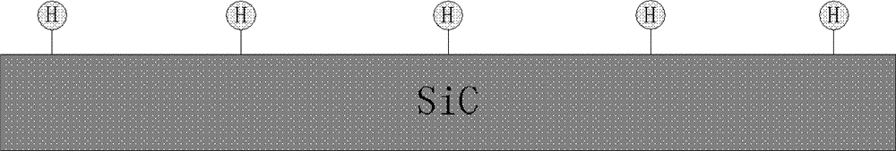
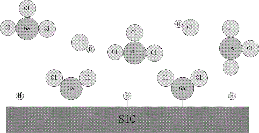
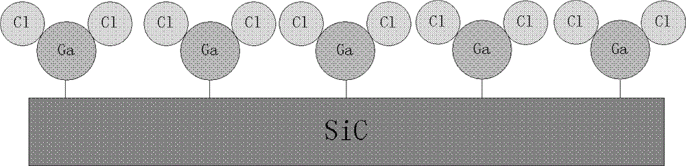
[0020] see figure 1 , a method for growing a gallium nitride thin film using an ALD device provided in an embodiment of the present invention includes:

[0021] Step 101, treating the surface of the silicon carbide substrate with a standard solution and hydrofluoric acid to form a silicon-hydrogen bond on the surface of the silicon carbide substrate, such as figure 1 As shown, wherein, the standard solution refers to: No. 1 liquid, concentrated sulfuric acid: hydrogen peroxide = 4: 1; No. 2 liquid, ammonia water: pure water: hydrogen peroxide = 1: 5: 1; No. 3 liquid, hydrochloric acid: hydrogen peroxide: pure water = 1:1:6; placing the silicon carbide substrate after the hydrogenation treatment in the reaction chamber of the atomic layer deposition equipment;

[0022] Step 102, turn on the atomic layer deposition equipment, adjust the working parameters, and achieve the working environment required for the experiment; first pass nitrogen gas into the reaction chamber of the a...


PUM

PropertyMeasurementUnit
poweraaaaaaaaaa

Abstract

Disclosed is a method for using an ALD device to grow a gallium nitride film, comprising: step 10: treating the surface of a silicon carbide liner by using a standard liquid and hydrofluoric acid, and placing the silicon carbide liner in a reaction cavity of an atom layer deposition device; step 20: piping a gallium source gas into the reaction cavity of the atom layer deposition device, the gallium source gas acting as a first reaction precursor source and being chemically absorbed to the surface of the silicon carbide liner, and gallium atoms in the gallium source gas being absorbed to the silicon carbide liner; and step 30: gallium atoms absorbed on the silicon carbide liner reacting with a second reaction precursor, which is ionized, with the assistance of hydrogen until the gallium atoms on the surface of the silicon carbide liner are completely consumed. The step 20 and the step 30 are repeated, so that a gallium nitride film is formed on the surface of the silicon carbide liner. In the method provided by the present invention, nitrogen is uniformly doped in the entire structure, the content of the doped nitrogen is high, and the structure of the film is complete.

Description

technical field [0001] The invention relates to the preparation of gallium nitride materials, in particular to a method for growing gallium nitride thin films with ALD equipment. Background technique [0002] The research and application of GaN materials is the frontier and hotspot of semiconductor research at present. It is a new type of semiconductor material for the development of microelectronic devices and optoelectronic devices, and it is the basis for the development of the LED industry. GaN material has a wide direct bandgap, high thermal conductivity and breakdown electric field, small dielectric constant, strong radiation resistance, and good chemical stability (almost not corroded by any acid), it is used in optoelectronics, high temperature and high power devices And high-frequency microwave device applications have broad prospects. In the LED industry, GaN materials with a complete structure and matching crystal constants directly affect the performance of LEDs...

Claims


Application Information

Patent Timeline
Patent Type & Authority Patents(China)
IPC IPC(8): C23C16/34C23C16/44
CPCC23C16/45534C30B29/406C23C16/303C23C16/0227C30B25/02
Inventor 饶志鹏万军夏洋陈波李超波石莎莉李勇滔李楠
Owner INST OF MICROELECTRONICS CHINESE ACAD OF SCI
Why Eureka
Try Eureka