

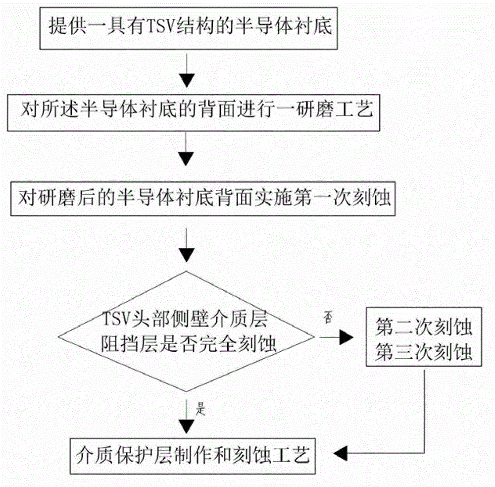
A kind of outcropping process on the back of tsv
A process and technology on the back, applied in the field of microelectronics, can solve problems such as low efficiency, large TTV, scratches, cracks, etc.
- Summary
- Abstract
- Description
- Claims
- Application Information
AI Technical Summary
Problems solved by technology
Method used
Image

Examples
Embodiment 1
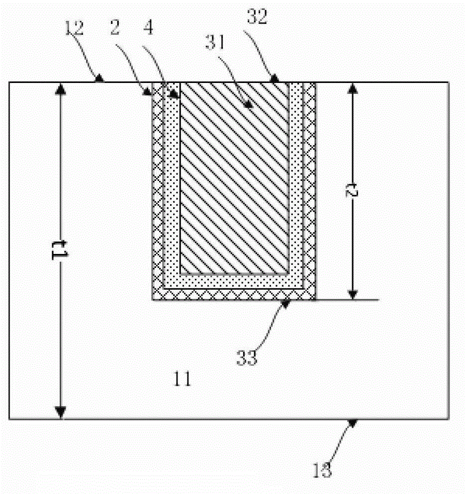
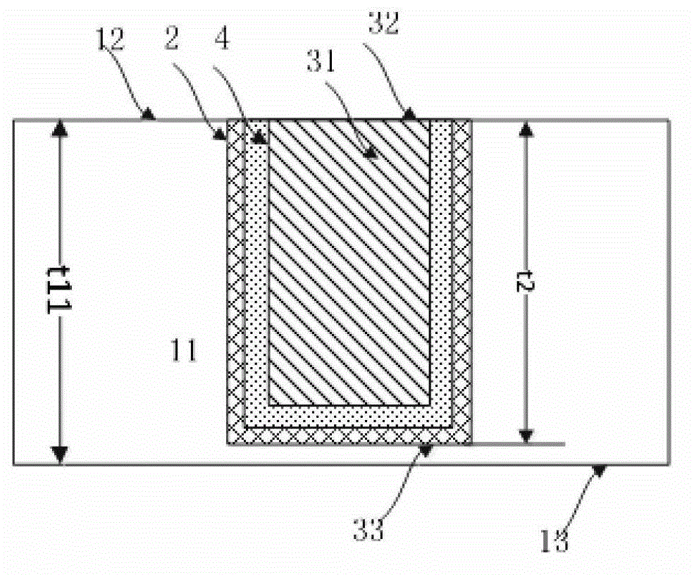
[0049] See Figures 2A-2G ,Should Figures 2A-2G It is a product structure diagram corresponding to each step in the first embodiment of the present invention. The meanings represented by the marks in the figure are as follows: 11 is the substrate (optionally, the substrate 11 is a silicon wafer (silicon wafer), silicon dioxide substrate (glass) or SiC), 12 is the front side of the substrate, 13 is the back side of the substrate, 2 is the dielectric layer (which can be silicon dioxide, silicon nitride or polymer), 31 is the TSV hole, 32 is the TSV hole, 33 is the bottom of the TSV hole (that is, the position of the subsequent outcrop), and 4 is Barrier layer (could be titanium, titanium nitride, tantalum or tantalum nitride, etc.). 51 is the dielectric protection layer (PI, BCB or POB, etc.), 52 is the final exposed TSV head, which can be directly interconnected with other devices, t1 is the initial thickness of the substrate, t11 is the thickness of the substrate after thin...
Embodiment 2
[0057] See Figures 3A-3F , Figures 3A-3F It is a device structure diagram corresponding to each step in the second embodiment of the present invention. The meanings of the marks in the diagram are as follows: 11 is the substrate (silicon wafer, glass, SiC), 12 is the front side of the substrate, 13 is the back side of the substrate, and 2 is the dielectric layer (which can be silicon dioxide, silicon nitride etc.), 31 is the TSV hole, 32 is the TSV hole, 33 is the bottom of the TSV hole (that is, the position of the subsequent outcrop), and 4 is the barrier layer (it can be titanium, titanium nitride, tantalum, tantalum nitride, etc.). 51 is the dielectric layer (PI, BCB, POB, etc.), 52 is the final exposed TSV head, which can be directly interconnected with other devices, etc., t1 is the initial thickness of the substrate, t11 is the thickness of the thinned substrate, and t12 is the second The substrate thickness after the first wet etching, t13 is the substrate thicknes...
PUM
 Abstract
Description
Claims
Application Information