

Semiconductor inks, films, coated substrates and methods of preparation
A technology of ink and substrate, which is applied in semiconductor/solid-state device manufacturing, semiconductor devices, ink, etc., and can solve problems such as severe toxicity
- Summary
- Abstract
- Description
- Claims
- Application Information
AI Technical Summary
Problems solved by technology
Method used
Image

Examples
preparation example Construction
[0196] Preparation of Inorganic Matrix : The inorganic matrix can be prepared by standard methods known in the art for the preparation of inorganic semiconductors, inorganic insulators and their precursors, and can be mixed with microparticles by methods similar to those described above. For example, containing SiO 2 The inorganic matrix or its precursor can be made of SiO 2 Sol-gel precursor prepared; contains Cu 2 ZnSn(S,Se) 4 The inorganic matrix or its precursors can be prepared as described above using molecular precursors; and contain Cu(In,Ga)(S,Se) 2 The inorganic matrix of or its precursors can be prepared from inks comprising CIGS / Se molecular precursors comprising:
[0197] i) a copper source selected from the group consisting of copper complexes of organic ligands based on nitrogen, oxygen, carbon, sulfur and selenium, copper sulfide, copper selenide, and mixtures thereof;
[0198] ii) a source of indium selected from indium complexes of organic ligands based...
example
[0256] review
[0257] Material : All reagents were purchased from Aldrich (Milwaukee, WI), Alfa Aesar (Ward Hill, MA), TCI (Portland, OR), Strem (Newburyport, MA) or Gelest (Morrisville, PA). The solid reagent was used without further purification. Liquid reagents not packaged under an inert atmosphere were degassed by bubbling the liquid through with argon for 1 hour. Anhydrous solvents were used for the preparation of all formulations and for all cleaning procedures performed in the dry box. Solvents were purchased in anhydrous form from Aldrich or Alfa Aesar, or purified by standard methods (e.g. Pangborn, A.G. et al., "Organometallics", 1996, 15, 1518-1520) and stored in a dry box over activated molecular sieves .
[0258] Formulation and coating preparation : The substrate (SLG slide) was sequentially washed with aqua regia, Cleaned with water and isopropanol, dried at 110 °C, and coated on the uneven surface of the SLG substrate. All formulations and coating...
example 1
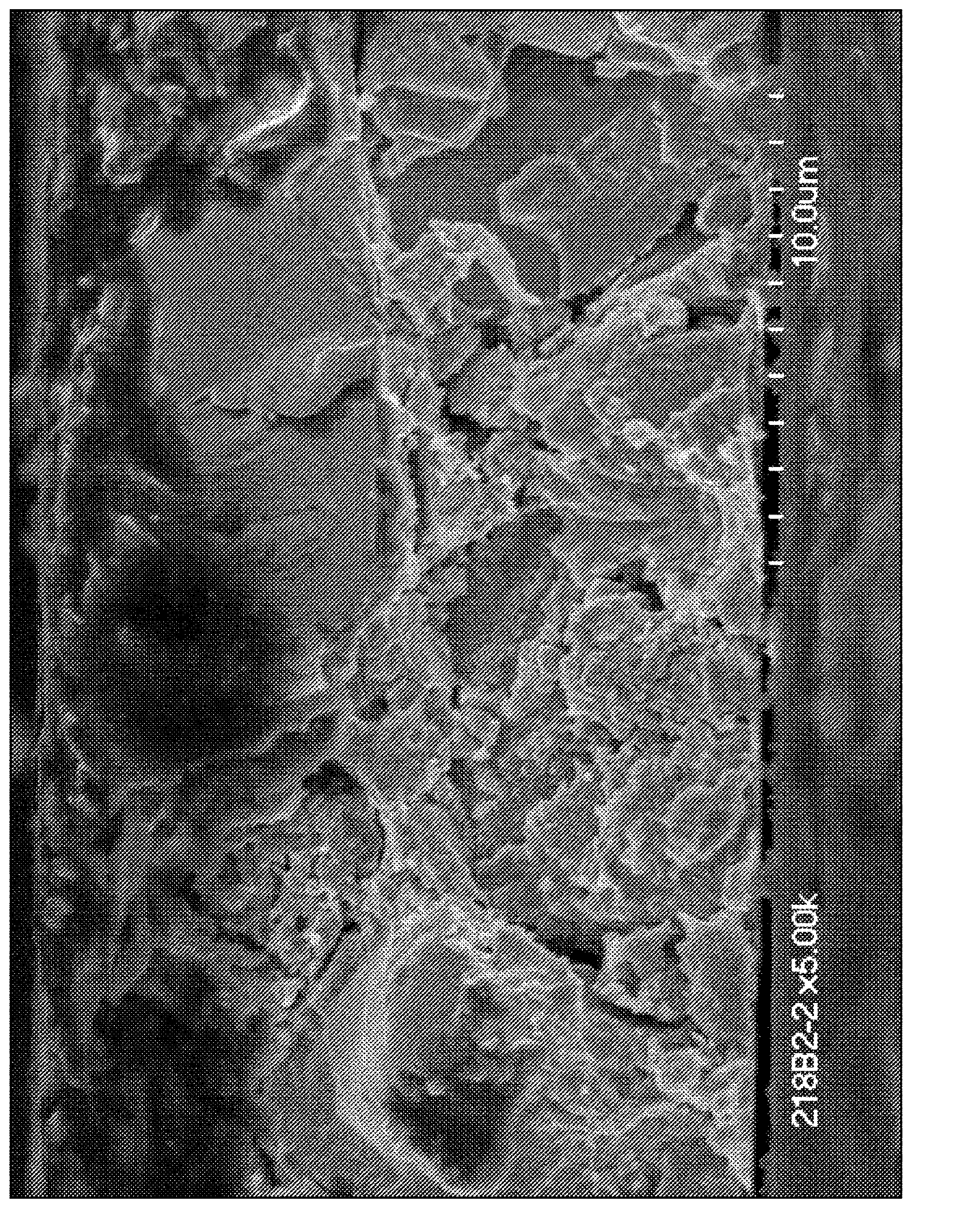
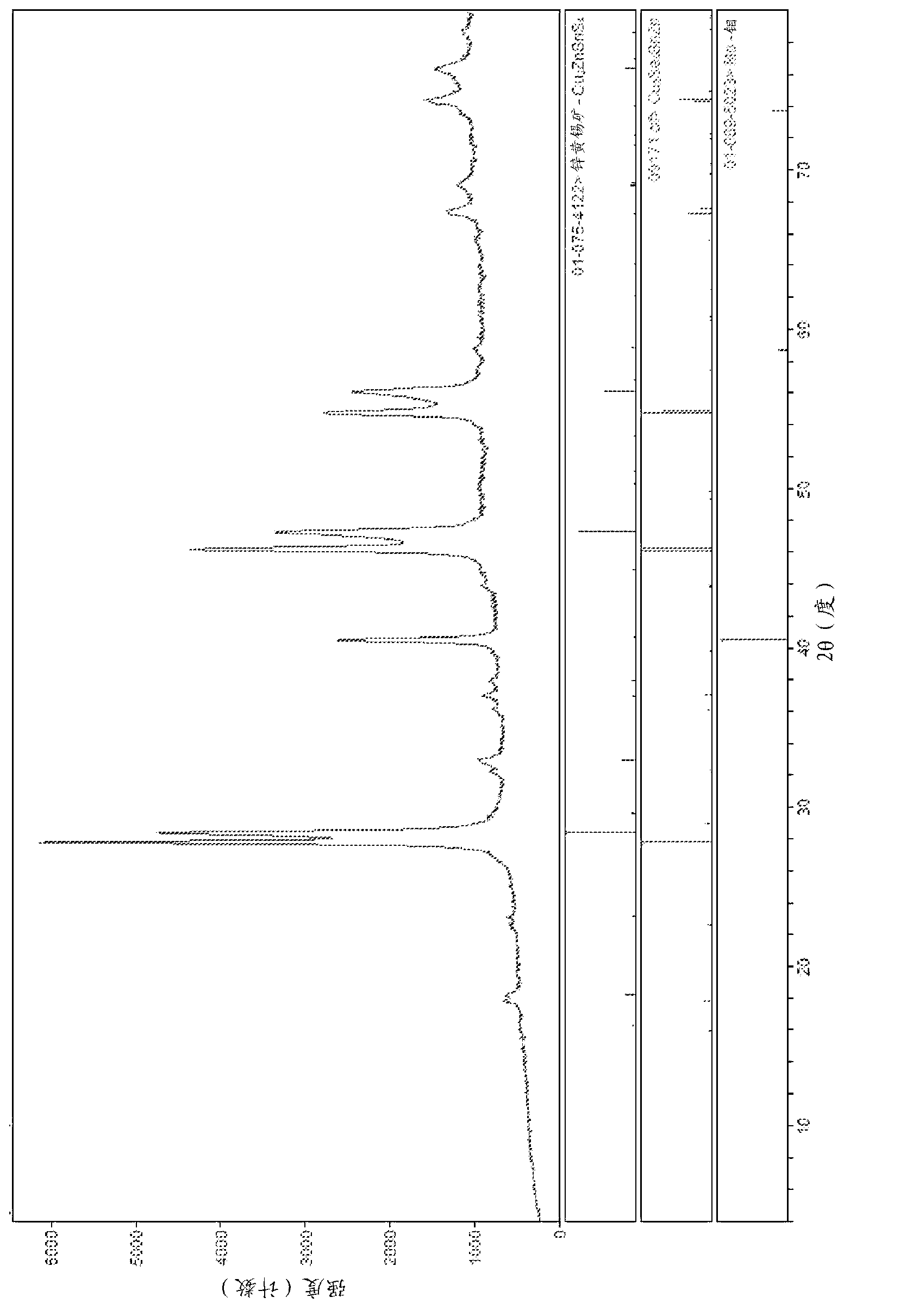
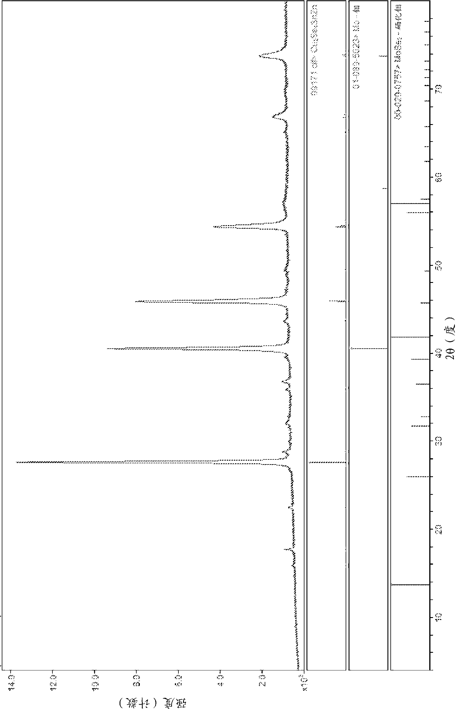
[0280] Example 1 shows the preparation of inks from the combination of molecular precursors prepared as described above and sieved CZTS crystallites. Active photovoltaic devices were fabricated from ink annealed films in Example 1A. The SEM cross-section of the film is shown in figure 1 , and demonstrate the presence of large microcrystalline domains (approximately 10 micron in size) embedded in a dense matrix. In Example IB, an annealed film was made from an ink comprising the molecular precursor of Example 1 in combination with CZTS particles made by the aqueous route. XRD of the annealed film ( figure 2 ) indicates the presence of CZTS and CZTS / Se, and is consistent with CZTS particles embedded in the CZTS / Se matrix. In Example 1C, XRD ( image 3 ) Only CZTS / Se was observed for films made from inks containing combinations of the molecular precursors of Example 1 and sieved CZTS crystallites. However, the EDX data for the region centered on the particle and the matrix ...
PUM
| Property | Measurement | Unit |
|---|---|---|
| boiling point | aaaaa | aaaaa |
| energy | aaaaa | aaaaa |
| boiling point | aaaaa | aaaaa |
Abstract
Description
Claims
Application Information