Substrate with transparent conductive oxide film

A transparent substrate and oxide film technology, applied in semiconductor devices, circuits, photovoltaic power generation, etc., can solve problems such as low conversion efficiency and short-circuit current reduction, and achieve the effects of suppressing reflection, suppressing contact resistance, and improving photoelectric conversion efficiency

Inactive Publication Date: 2013-09-11
ASAHI GLASS CO LTD
View PDF4 Cites 0 Cited by
  • Summary
  • Abstract
  • Description
  • Claims
  • Application Information

AI Technical Summary

Problems solved by technology

As a result, there is a short circuit current (J SC ) reduction,

Method used


Image

  • Substrate with transparent conductive oxide film
  • Substrate with transparent conductive oxide film
  • Substrate with transparent conductive oxide film

Examples


Embodiment

[0129] Hereinafter, although an Example demonstrates this invention in detail, this invention is not limited to these Examples.

[0130] In the examples, a film-coated substrate was fabricated according to the procedure shown below, and the photoelectric conversion characteristics of a module formed of a thin-film photoelectric conversion element fabricated using the film-coated substrate were evaluated.

[0131] However, among Examples 1 to 7 shown below, Examples 1 to 4 are examples, and Examples 5 to 7 are comparative examples.

example 1

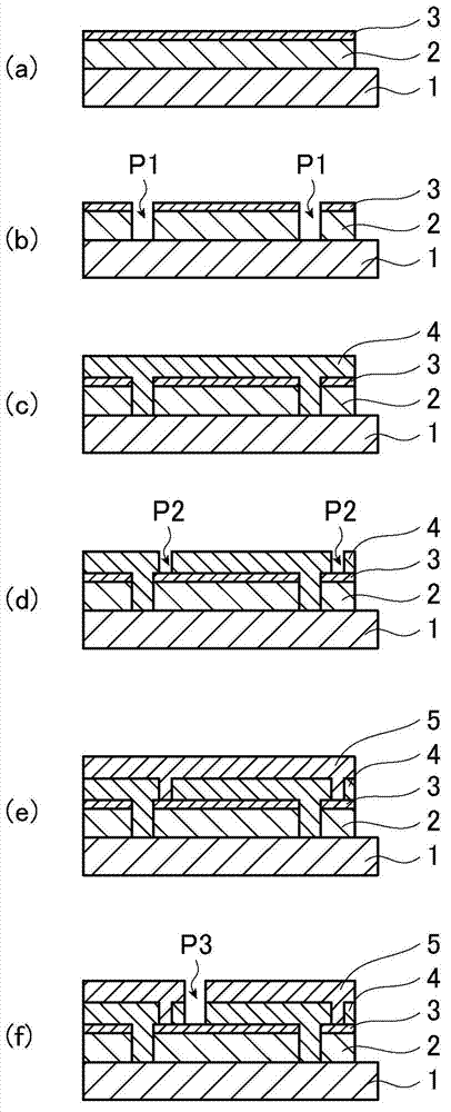
[0133] As a substrate, a soda lime silicate glass substrate (300mm×300mm×3.9mm) with an antireflection film laminated with a titanium oxide layer (thickness 10nm) and a silicon oxide layer (thickness 30nm) was used. A fluorine-doped tin oxide film was formed as the first film by an atmospheric pressure CVD method. The procedure for forming a fluorine-doped tin oxide film by atmospheric pressure CVD is as follows.

[0134] The temperature of the substrate was raised to 550° C. with an electric heater, and a source gas containing tin tetrachloride, water vapor, and hydrogen fluoride as raw materials was purged from a nozzle to form a first film as a fluorine-doped tin oxide film with a thickness of 700 nm.

[0135] The sheet resistance of the formed first film was measured by the DC 4-probe method, and as a result, the sheet resistance was 9Ω / □. In addition, when the molar ratio F / Sn of the first film was measured by secondary ion mass spectrometry (SIMS), the molar ratio F / Sn ...

example 2~ example 7

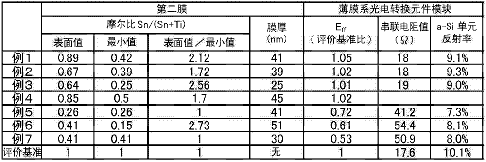
[0162] The same procedure as in Example 1 was carried out except that the raw material composition and supply amount of the raw material mixed gas were adjusted so that the film thickness of the second film and the molar ratio Sn / (Sn+Ti) were the values ​​shown in the following table. The results are shown in the following tables. Blank columns in the table indicate no measurement data.

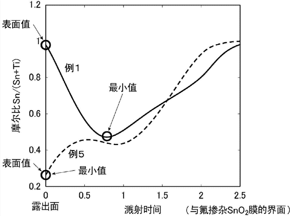
[0163] Here, regarding Examples 2 to 4 and 6, the surface value of the molar ratio Sn / (Sn+Ti) existing on the surface of the second film similarly to Example 1 is the molar ratio Sn / (Sn+Ti) within the total film thickness of the second film The maximum value of Sn+Ti) and the minimum value of the molar ratio Sn / (Sn+Ti) exist inside the second film. On the other hand, example 5 such as figure 1 As shown, there is a minimum of the molar ratio Sn / (Sn+Ti) at the surface of the second film. Fig. 7 also has the minimum value of the molar ratio Sn / (Sn+Ti) at the surface of the second film as in ...


PUM

PropertyMeasurementUnit
Film thicknessaaaaaaaaaa

Abstract

The invention relates to a substrate with a transparent conductive oxide film. The substrate is successively laminated by a transparent matrix, a first film and a second film on the matrix, wherein the second film is contacted with the first film; the thickness of the second film is 10-100 nm; the first film is a transparent conductive oxide film with stannic oxide as a main component; at least the contact surface of the first film and the second film is fluorine-doped stannic oxide with a molar ratio of fluorine to stannic being 0.0001-0.09; the second film is a transparent conductive oxide film containing titanium oxide and stannic oxide; a molar ratio of stannic to a total amount of stannic and titanium changes in the film thickness direction from the surface of the second film to the surface contacted with the first film; and when a maximum value of the molar ratio in a range from the surface of the second film to a depth of 5 nm along the film thickness direction is taken as a surface value; and a minimum value of the molar ratio with a total thickness in the film thickness direction of the second film is taken as the minimum value, the surface value of the second film is higher than 0.45 and is more than 1.2 times that of the minimum value.

Description

technical field [0001] The present invention relates to filmed substrates having transparent conductive oxide films. The substrate with a film of the present invention is suitable as a substrate with a transparent conductive oxide film for producing a thin-film photoelectric conversion device as a thin-film solar cell. Background technique [0002] Thin-film photoelectric conversion devices that are thin-film solar cells include amorphous silicon (a-Si)-based, polycrystalline silicon-based, and the like depending on the type of photoelectric conversion layer (semiconductor layer). In these thin-film silicon-based solar cells, a transparent conductive oxide film is used as a transparent electrode layer on the light-incident side thereof. This transparent conductive oxide film is required to have low resistance and high transparency in order to improve photoelectric conversion efficiency. As a transparent conductive oxide film, it is known that it contains 0.01 to 4 mol% of ...

Claims


Application Information

Patent Timeline
IPC IPC(8): H01L31/0236H01L31/0392
CPCY02E10/50
Inventor 东诚二增茂邦雄
Owner ASAHI GLASS CO LTD
Why Eureka
Try Eureka