Graphene high-frequency nanomechanical resonator based on flexible substrate and preparing technology of graphene high-frequency nanomechanical resonator

A flexible substrate and preparation technology, applied in the direction of electrical components, impedance networks, etc., can solve the problems of improving and limiting the electromechanical resonance frequency of graphene beam nanometers, and achieve the effect of increasing the resonance frequency

Inactive Publication Date: 2013-09-11
UNIV OF ELECTRONIC SCI & TECH OF CHINA
View PDF2 Cites 30 Cited by
  • Summary
  • Abstract
  • Description
  • Claims
  • Application Information

AI Technical Summary

Problems solved by technology

At present, research on graphene nanoelectromechanical systems (NEMS) is mainly concentrated on hard substrates. Due to the influe

Method used


Image

  • Graphene high-frequency nanomechanical resonator based on flexible substrate and preparing technology of graphene high-frequency nanomechanical resonator
  • Graphene high-frequency nanomechanical resonator based on flexible substrate and preparing technology of graphene high-frequency nanomechanical resonator

Examples


Embodiment 1

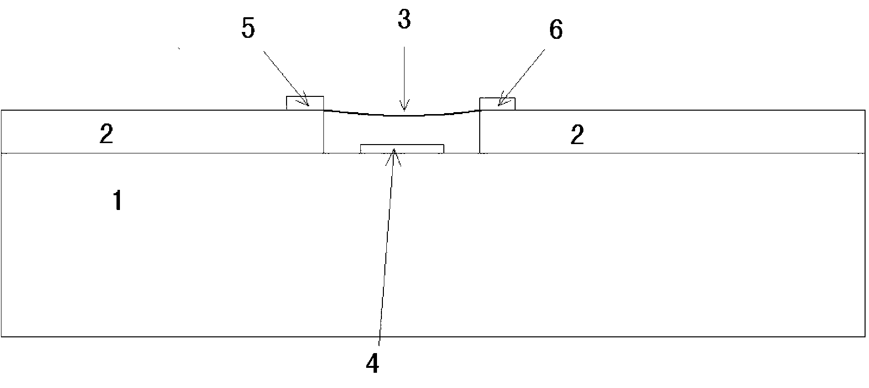
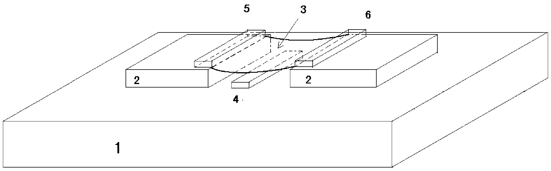
[0034] The preparation technology of the high-frequency graphene nano-electromechanical resonator based on flexible substrate of the present invention, its operating steps are as follows:

[0035] Step 1: Spin-coat photoresist (PMMA) on polyethylene naphthalate (PEN) flexible substrate 1, and use electron beam etching to make the shape of gate metal electrode 4, with a gate length of 300nm and a gate width of 500nm ;

[0036] Step 2: Evaporate a layer of titanium metal with a thickness of 1 nm and a layer of gold-platinum alloy with a thickness of 30 nm on the surface of the flexible substrate 1 in step 1 by evaporation; then remove the excess photoresist and the metal attached to it, leaving only A patterned gate metal electrode 4 on the lower flexible substrate 1;

[0037] Step 3: Deposit a layer of silicon dioxide (SiO 2 ) dielectric layer 2;

[0038] Step 4: Spin-coat photoresist (PMMA) on the prepared graphene wafer, and then put the graphene wafer into iron nitrate (F...

Embodiment 2

[0046] In this example, the flexible material polyethylene naphthalate (PEN) used in Example 1 is replaced by polyethylene terephthalate (PET), and plasma-enhanced chemical vapor deposition is used on the flexible substrate 1 (PECVD) deposited a layer of silicon dioxide (SiO 2 ) Dielectric layer 2, the width of the graphene channel is 2000nm; other process steps and process conditions are the same as in Example 1, and a graphene-based high-frequency and high-Q nanoelectromechanical resonator based on a flexible substrate can also be prepared.


PUM

PropertyMeasurementUnit
Thicknessaaaaaaaaaa
Widthaaaaaaaaaa

Abstract

The invention relates to a graphene high-frequency nanomechanical resonator based on a flexible substrate and a preparing technology of the graphene high-frequency nanomechanical resonator and belongs to the technical field of communication electronic elements. According to the technology, the shape of a required gate electrode is etched on the flexible substrate. A metal layer is evaporated on the surface of the flexible substrate. Silicon dioxide sedimentation is conducted on the flexible substrate. Graphene is transferred to the portion right above the gate electrode and photoresist is painted on the gate electrode in a spiral mode. Titanium, platinum and gold are evaporated on a channel of the graphene so as to serve as a source electrode and a drain electrode. Finally, a whole element is coated with photoresist and the graphene high-frequency Q nanomechanical resonator of the flexible substrate can be obtained after processing. The structure of the graphene high-frequency Q nanomechanical resonator comprises the flexible substrate, a medium layer, the gate electrode and a graphene girder in a sequentially laminated mode. The source electrode and the drain electrode are located at the two sides of the graphene girder. The graphene high-frequency nanomechanical resonator is a microwave element which has the advantages of being high in frequency, high in quality factors, light, thin, soft, good in shock resistant performance and low in cost.

Description

technical field [0001] The invention relates to a communication electronic component, in particular to a graphene high-frequency nano-electromechanical resonator based on a flexible substrate and a preparation process thereof, belonging to the technical field of communication electronic components. Background technique [0002] As a two-dimensional nanomaterial with a single atomic layer, the carriers in graphene are Dirac fermions, which have good linear dispersion characteristics. Compared with traditional silicon, gallium arsenide and other semiconductor materials, graphene has more High carrier mobility, electron saturation rate and thermal conductivity. At the same time, graphene has strong mechanical strength and toughness, the tensile strength is more than ten times that of steel, and it can still maintain its performance when cut to less than ten nanometers. It is used as a high-speed, high-Q, miniaturized nano-electromechanical resonator. Ideal material. At presen...

Claims


Application Information

Patent Timeline
IPC IPC(8): H03H9/15H03H3/02
Inventor 徐跃杭李欧鹏孙岩徐锐敏
Owner UNIV OF ELECTRONIC SCI & TECH OF CHINA
Why Eureka
Try Eureka