Built-in self-test structure and method for on-chip network resource node storage device

A technology of built-in self-test and resource node, applied in the field of built-in self-test structure of on-chip network resource node memory, can solve problems such as the number of users cannot exceed one pair, the bus structure address space is limited, and the communication efficiency is low, so as to save The effect of test cost, shortened test time, and high fault coverage

Active Publication Date: 2013-09-18
GUILIN UNIV OF ELECTRONIC TECH
View PDF4 Cites 15 Cited by
  • Summary
  • Abstract
  • Description
  • Claims
  • Application Information

AI Technical Summary

Problems solved by technology

[0003] 1. The address space of the bus structure is limited, which leads to the problem of poor scalability
[0004] 2. The bus structure adopts time-sharing communication, which leads to low communication efficiency. Multiple users on the bus share bus resources at the same time. The number of users communicating on a bus at a certain time cannot exceed one pair
[0005] 3. The power consumption and area of ​​the bus structure due to the use of a global synchronous communication mechanism
[0014] At present, there have been a large number of built-in self-test designs for SoC memories with bus structures, but there have been no reports on the use of built-in self-test methods for memories in NoC systems.

Method used


Image

  • Built-in self-test structure and method for on-chip network resource node storage device
  • Built-in self-test structure and method for on-chip network resource node storage device
  • Built-in self-test structure and method for on-chip network resource node storage device

Examples


Embodiment Construction

[0050] Embodiment of built-in self-test structure of on-chip network resource node memory

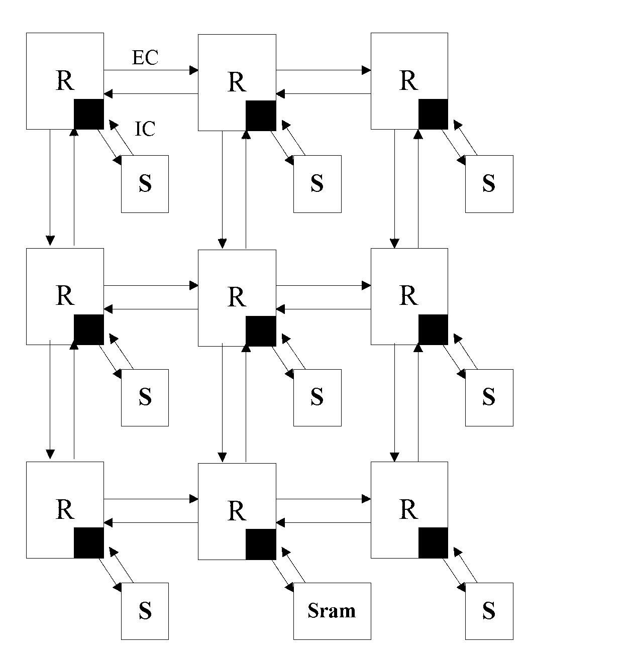
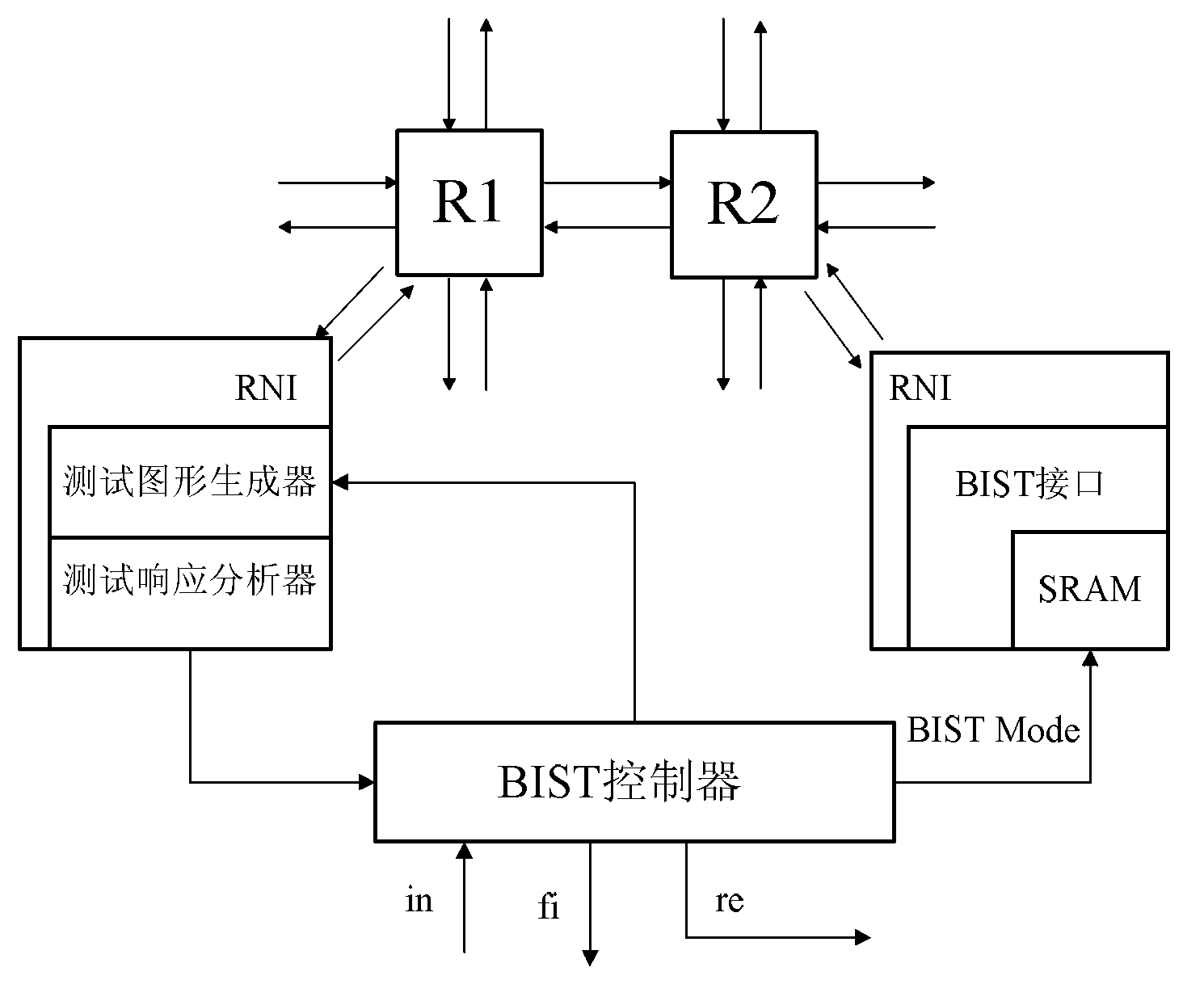
[0051] The on-chip network used in the built-in self-test structure embodiment of this on-chip network resource node memory is based on FPGA chips, such as figure 1 As shown, 3×3 routers R are connected to each other by external channels EC, forming a router network with a regular 2-dimensional grid (2D-Mesh) topology. The routers in the NoC adopt a wormhole data exchange mechanism based on virtual channel technology. The algorithm adopts the source routing algorithm. Each router is connected to the resource node through the resource network interface. The off-chip general-purpose memory SRAM connected to one router R2 through the resource network interface is the resource node memory to be tested. The resource node memory to be tested is represented by SRAM below. The resource network interface is a bidirectional data flow interface.

[0052] The built-in self-test structure of the re...


PUM


Abstract

The invention discloses a built-in self-test structure and method for an on-chip network resource node storage device. The built-in self-test structure comprises a built-in self-test (BIST) controller arranged on a field programmable gate array (FPGA) chip, a resource network interface and a BIST interface which are embedded into corresponding routers, a test pattern generator and a test response analyzer, wherein the BIST controller is connected with external test equipment through an external interface. The built-in self-test method comprises the following steps that: the external test equipment sends an instruction start test program to the BIST controller; the BIST controller sends an enabling signal and a state selection signal to each test module according to a March C+ test algorithm program, performs read-write operation on each address of a static random access memory (SRAM) under each test state, and stops sending the signals if failures are found out. A test result is sent to the external test equipment. According to the built-in self-test structure and method, the test time is reduced by 50 percent; a routing network of a network operation center (NoC) is reused as a test data route; data transmission is reliable and safe; a chip area is low in expense; the failure coverage rate is high.

Description

technical field [0001] The invention relates to the technical field of Network-on-chip (NoC) testing, in particular to a built-in self-testing structure and a self-testing method of a network-on-chip (NoC) resource node memory. Background technique [0002] With the advancement of semiconductor technology and the continuous improvement of SoC (System-on-chip, SoC) technology, SoC technology has become the main design technology of integrated circuits in this century. However, its design method and architecture have exposed limitations, especially when the number of IP cores included in the SoC increases to tens of thousands, the existing SoC technology based on the bus structure is facing challenges in Huge challenges in terms of performance, power consumption, latency, and reliability. The problems that arise are specifically manifested in the following three aspects: [0003] 1. The address space of the bus structure is limited, which leads to the problem of poor scalabi...

Claims


Application Information

Patent Timeline
Patent Type & Authority Applications(China)
IPC IPC(8): G11C29/12
Inventor 许川佩陶意万春霆孙义军梁光发
Owner GUILIN UNIV OF ELECTRONIC TECH
Why Eureka
Try Eureka