Semiconductor stack and vertical cavity surface emitting laser
A technology of semiconductors and laminates, applied in the direction of semiconductor lasers, lasers, laser components, etc., can solve the problems of low thermal conductivity, high output, carrier density distribution is not considered, and achieve high carrier confinement effect Effect
- Summary
- Abstract
- Description
- Claims
- Application Information
AI Technical Summary
Problems solved by technology
Method used
Image
Examples
no. 1 example
[0040]A vertical cavity surface emitting laser is a semiconductor laser that has excellent wavelength controllability because its oscillation wavelength is determined by the film thickness of the mirror and the film thickness of the resonator. The emission wavelength is determined by the composition and film thickness control of the quantum well layer in the active layer. Therefore, it is possible to achieve wavelength stability and high efficiency relatively easily.
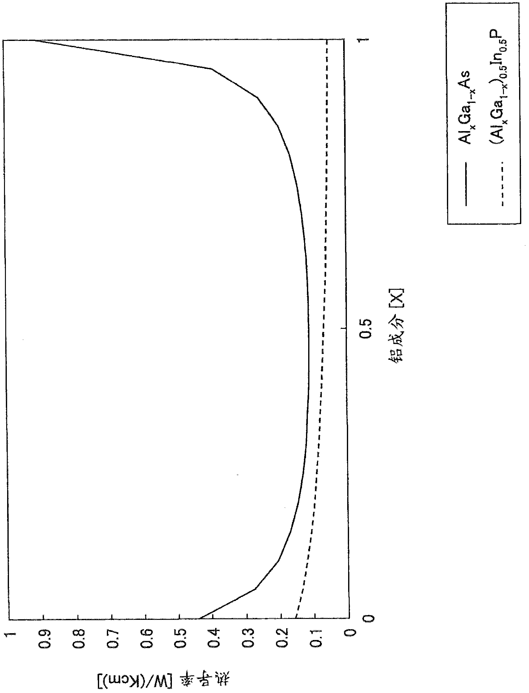
[0041] However, a relatively thick mirror must be provided between the active layer and the heat-radiating material. Therefore, the vertical cavity surface emitting laser has inferior thermal radiation characteristics compared to the edge emitting type laser, which causes the temperature of the quantum well layer to rise, resulting in characteristic degradation such as reduced output. Therefore, when aiming at high output, the material and film thickness of the configuration mirror should be fully considered. ...
no. 2 example
[0069] Next, a description will be given of a semiconductor laminated board according to a second embodiment. like Figure 5 As shown, the semiconductor laminated board in this embodiment has a structure different from that of the semiconductor laminated board in the first embodiment.
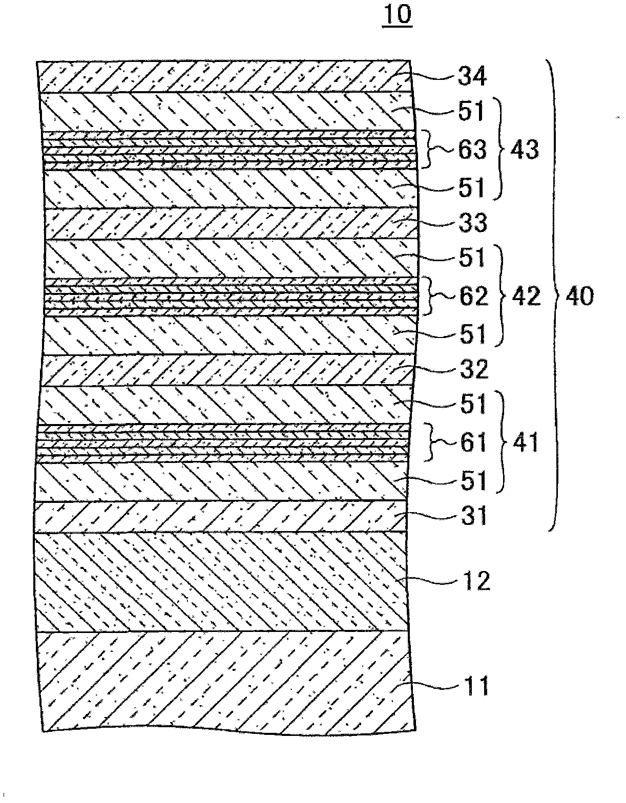
[0070] In this embodiment, in the semiconductor laminated board 10, a gallium arsenide (100) substrate formed at an angle of 15 degrees ((111) direction) is used as the substrate 11 on which 30 pairs of gallium arsenide / aluminum arsenide layers are The semiconductor DBR12 is formed by stacking. A spacer layer 113 is formed of gallium arsenide on the semiconductor DBR12, on which the first carrier blocking layer 131, the first active layer 41, the second carrier blocking layer 132, the second active layer 42, the second The three carrier blocking layers 133, the third active layer 43, and the fourth carrier blocking layer 134 are formed in this order. It should be noted that, in this embodime...
no. 3 example
[0085] (Vertical cavity surface emitting laser device)
[0086] Here, a third embodiment will be described. In the present embodiment, a vertical cavity surface emitting laser device having an oscillation wavelength in the 980 nm range using the semiconductor laminated plate according to the first or second embodiment will be described.
[0087] like Figure 7 As shown, the vertical cavity surface emitting laser device in this embodiment is formed on a type of semiconductor substrate 200, which is an inclined substrate inclined in the plane direction, on which a buffer layer 201, a lower layer semiconductor DBR202, The active layer 205 and the upper semiconductor DBR 207. Also, on top of the upper semiconductor DBR 207, a contact layer 209 is formed. By removing part of the contact layer 209 , an upper semiconductor DBR 207 , an active layer 205 and a convex mesa 220 are formed. A current confinement layer 208 is formed in the upper semiconductor DBR 207, which is oxidized...
PUM
 Abstract
Description
Claims
Application Information


