Sliding friction nano generator and power generation method
A nanometer generator and sliding friction technology, applied in the direction of friction generators, etc., can solve the problems of power supply components that cannot be used for microelectronic devices, large generator volume, complex structure, etc., and achieve simple structure, small size, and wide application Effect
- Summary
- Abstract
- Description
- Claims
- Application Information
AI Technical Summary
Problems solved by technology
Method used
Image
Examples
Embodiment 1
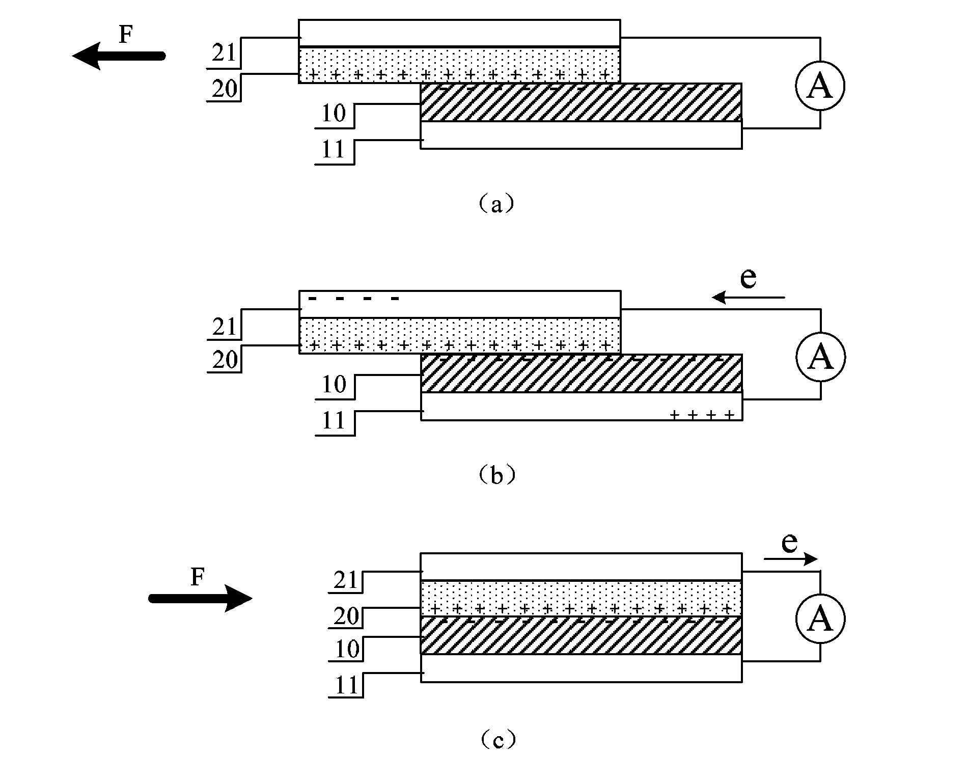
[0097] The first conductive element adopts a metal copper film layer with a thickness of 100nm, the first friction layer adopts a Teflon (polytetrafluoroethylene) film with a thickness of 25 microns, and the second friction layer adopts a metal aluminum film layer with a thickness of 100nm. The second conductive element is an indium tin oxide ITO thin film, and the macroscopic size of these film layers is 5 cm×7 cm. The metal copper film layer and the ITO film layer are connected to the ammeter through wires, and the Teflon film and the metal aluminum film are placed in contact with each other completely overlapping, and then the metal copper film layer is repeatedly pushed and pulled with fingers with insulating gloves to make the Teflon film Periodic reciprocating relative sliding occurs between the film layer and the metal aluminum film layer, and there is a short-circuit current output on the ammeter, indicating that the generator is working normally. The generator can dri...
Embodiment 2
[0100] Polydimethylsiloxane (English abbreviated as PDMS) with a thickness of 50 microns and 3cm×8cm is used as the first friction layer 10, and a silicon wafer with the same macroscopic size is used as the second friction layer, and the silicon wafer is spin-coated A layer of photoresist is applied, and a square window array with a side length of micron or submicron is formed on the photoresist by photolithography; the silicon wafer after photolithography is chemically etched by hot potassium hydroxide, A pyramid-shaped array of recessed structures is formed at the window. When the silicon wafer and PDMS are in contact with each other under the action of external force and relatively slide, due to the good elasticity of PDMS, it can enter and fill the concave structure on the surface of the silicon wafer, thereby increasing the distance between the silicon wafer and the silicon wafer. The frictional contact area can obtain better electrical output effect.
Embodiment 3
[0102] In this embodiment, on the basis of embodiment 1, only the polytetrafluoroethylene film is modified, and the others are the same as in embodiment 1, and will not be repeated here. Nanowire arrays were prepared by inductively coupled plasma etching on the surface of the polytetrafluoroethylene film. First, about 10 nanometers of gold was deposited on the surface of the polytetrafluoroethylene film with a sputtering device, and then the polytetrafluoroethylene film was placed in an inductor. In the coupled plasma etching machine, etch the side on which the gold is deposited, and pass O 2 , Ar and CF 4 Gas, the flow rate is controlled at 10sccm, 15sccm and 30sccm respectively, the pressure is controlled at 15mTorr, the working temperature is controlled at 55°C, the plasma is generated with a power of 400 watts, and the plasma is accelerated with a power of 100 watts for about 5 minutes of etching , to obtain a polymer polytetrafluoroethylene nanorod array with a length of...
PUM
| Property | Measurement | Unit |
|---|---|---|
| Thickness | aaaaa | aaaaa |
| Thickness | aaaaa | aaaaa |
| Length | aaaaa | aaaaa |
Abstract
Description
Claims
Application Information


