Micropore thin film micro-fluidic chip as well as preparation method and application thereof

A technology of microfluidic chips and microporous films, applied in chemical instruments and methods, containers used in laboratories, and analysis through chemical reactions of materials, etc., can solve complex technology participation in production, increase production costs, and operators Harm and other issues, to achieve good environmental compatibility, low cost, and less harmful effects

Inactive Publication Date: 2013-10-30
INST OF CHEM CHINESE ACAD OF SCI
View PDF6 Cites 7 Cited by
  • Summary
  • Abstract
  • Description
  • Claims
  • Application Information

AI Technical Summary

Problems solved by technology

For example, in wet etching, hydrofluoric acid, nitric acid and ammonium fluoride will be used in large quantities, which will not only cause certain hazards to operators, but also cause related damage to the environment
Relevant heavy metals will be used in the metal coating process, which is also quite harmful to the human body
[0006] 2. Long production cy

Method used


Image

  • Micropore thin film micro-fluidic chip as well as preparation method and application thereof
  • Micropore thin film micro-fluidic chip as well as preparation method and application thereof

Examples


Embodiment 1

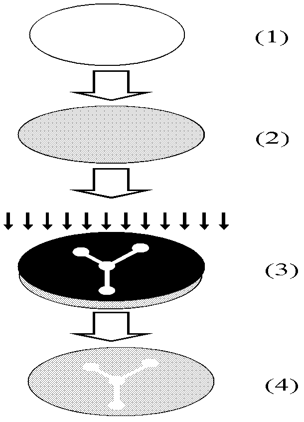
[0027] Embodiment 1, the making of nylon microporous film microfluidic chip

[0028] 1) if figure 1 Shown in (1), the nylon microporous film 1 that thickness is 100 μ m, porosity 70%, aperture is 0.45 μ m is soaked in the photoresist of positive-type ultraviolet photoresist 3 minutes, makes photoresist fully contact with film microporous film The holes are in contact with each other and filled, take it out and let it stand for 10 minutes, so that the excess photoresist on the film will drop naturally and be initially cured; The resist cures to form a hard photoresist film, such as figure 1 (2) shown.

[0029] 3) Use high-resolution printing technology to print channel graphics on black and white film with a printing resolution of 3657dpi; put a black mask close to the photoresist film for UV exposure, and the exposure ends after 10 minutes, using a mass percent concentration of 0.7 % sodium hydroxide aqueous solution washes off the UV positive photoresist after exposure to ...

Embodiment 2

[0033] Embodiment 2, the making of polypropylene microporous film microfluidic chip

[0034] 1) if figure 1 As shown in (1), the polypropylene microporous film 1 with a thickness of 150 μm, a porosity of 80%, and a pore diameter of 0.5 μm is soaked in the positive-type UV photoresist photoresist for 2 minutes, so that the photoresist is fully in contact with the film. Contact the micropores and fill them, take them out and let them stand for 15 minutes to allow the excess photoresist on the film to drip naturally and preliminarily cure; then place the incompletely cured film on an electric heating plate at 75°C and bake for 20 minutes. The photoresist cures to form a hard photoresist film, such as figure 1 (2) shown.

[0035] 3) Use high-resolution printing technology to print channel graphics on black and white film with a printing resolution of 3657dpi; put the black mask close to the photoresist film for UV exposure, and the exposure ends after 8 minutes, with a mass perc...


PUM

PropertyMeasurementUnit
Thicknessaaaaaaaaaa
Thicknessaaaaaaaaaa
Thicknessaaaaaaaaaa

Abstract

The invention discloses a micropore thin film micro-fluidic chip as well as a preparation method and an application thereof. The method comprises the following steps of: (1), utilizing a micropore thin film as a carrier, soaking in a photoresist standing and drying to from a photoresist thin film; and (2), enabling a mask to cover the photoresist thin film obtained in the step (1) so as to carry out exposure, finishing the exposure, dissolving the photoresist to obtain a micro-fluidic chip channel, and carrying out plasma treatment on the micro-fluidic chip channel to obtain the micropore thin film micro-fluidic chip. The chip of the method provided by the invention has the advantages that the manufacturing operation is simple and rapid, the material selection is novel and unique, the cost is low, the source is wide, and the chip is used for volume production; the operation steps can be finished in a routine laboratory, the applicability is strong, a chip manufacturing operation adopts conventional reagents such as a rare aqueous alkali, the corrosivity reagent is not used, and the environment compatibility is good.

Description

technical field [0001] The invention belongs to the technical field of microfluidic chips, and relates to a microporous film microfluidic chip, a preparation method and application thereof. Background technique [0002] The microfluidic analysis system that emerged with the development of microelectromechanical systems (MEMS) has been greatly developed since it appeared in the 1990s and has been widely used in various disciplines. Microfluidic analysis refers to a micro-full analysis system that uses micro-pipes as a network to connect various micro-functional units, and integrates analysis functions such as sampling, dilution, reagent addition, reaction, separation, and detection on the chip to the greatest extent. As the carrier of the microfluidic analysis system-microfluidic chip, its processing and production are greatly developed and researched as an important technology. [0003] Generally speaking, the processing technology of microfluidic chip includes wet etching,...

Claims


Application Information

Patent Timeline
IPC IPC(8): B01L3/00G01N33/48G01N21/78
Inventor 齐莉杨俊马会民
Owner INST OF CHEM CHINESE ACAD OF SCI
Why Eureka
Try Eureka