Silicon-based germanium laser device and method for manufacturing same

A laser, silicon-based technology, applied in the structure of optical waveguide semiconductors, etc., can solve the problems affecting the quality of germanium epitaxial layers, unable to achieve continuous operation, and immature polishing process, and achieve good current injection efficiency and ensure current injection efficiency. , reduce the effect of non-radiative recombination

Inactive Publication Date: 2013-12-04
INST OF SEMICONDUCTORS - CHINESE ACAD OF SCI
View PDF8 Cites 22 Cited by
  • Summary
  • Abstract
  • Description
  • Claims
  • Application Information

AI Technical Summary

Problems solved by technology

However, their laser is a vertical p-i-n structure, the germanium material is grown on a highly doped silicon substrate, and the germanium material is doped with a high concentration of n-type, which affects the quality of the germanium epitaxial layer; the doped layer and the electrode The absorption of light is not well avoided; it is necessary to adopt a complex and immature chemical mechanical polishing process for germanium materials, and the consistency of the device is not good; the lasing threshold of the device is too large, the life is very short, and continuous operation cannot be achieved

Method used


Image

  • Silicon-based germanium laser device and method for manufacturing same
  • Silicon-based germanium laser device and method for manufacturing same
  • Silicon-based germanium laser device and method for manufacturing same

Examples


Embodiment Construction

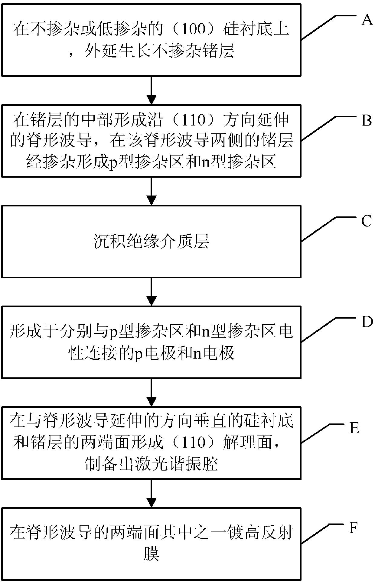
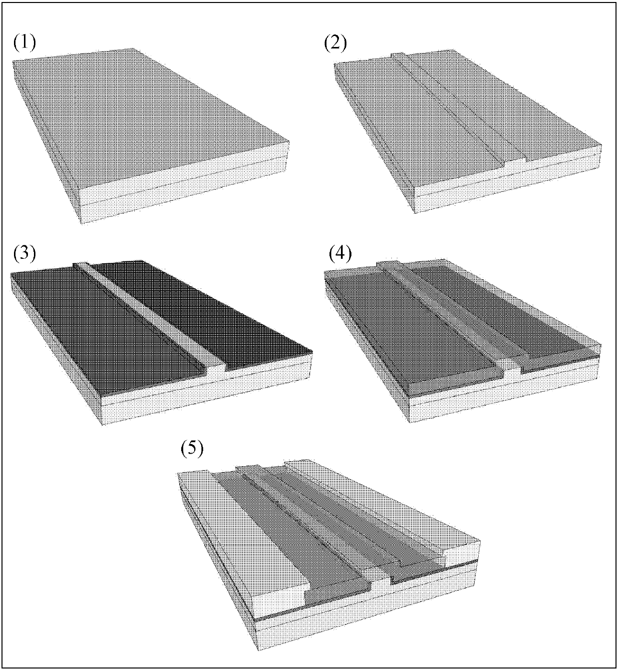
[0025] In order to make the object, technical solution and advantages of the present invention clearer, the present invention will be described in further detail below in conjunction with specific embodiments and with reference to the accompanying drawings. In the drawings or descriptions in the specification, similar or identical parts all use the same figure numbers. Implementations not shown or described in the accompanying drawings are forms known to those of ordinary skill in the art.

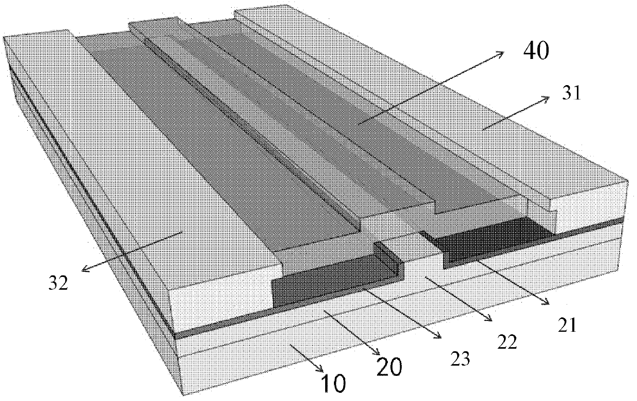
[0026] The invention provides a silicon-based germanium laser with a lateral p-i-n structure and a preparation method thereof. The whole device is manufactured by conventional semiconductor device technology, and has good compatibility with CMOS technology.

[0027] In an exemplary embodiment of the present invention, a germanium-on-silicon laser is provided. Please refer to figure 1 , the silicon-based germanium laser in this embodiment comprises: a silicon substrate 10; a germanium la...


PUM

PropertyMeasurementUnit
thicknessaaaaaaaaaa
thicknessaaaaaaaaaa
thicknessaaaaaaaaaa

Abstract

The invention provides a silicon-based germanium laser device and a method for manufacturing the same. The silicon-based germanium laser device comprises a silicon material, a germanium layer, a p-type doped region, an n-type doped region, an insulating dielectric layer, a p electrode and an n electrode; the silicon material is provide with corresponding crystal orientation; the germanium layer epitaxially grows on the silicon material and comprises a germanium ridge waveguide, the germanium layer is etched to form the germanium ridge waveguide, and the germanium ridge waveguide forms all or partial laser resonant cavities; the p-type doped region and the n-type doped region are positioned on two sides of the germanium ridge waveguide; the p-type doped region, the germanium ridge waveguide and the n-type doped region form a transverse p-i-n diode structure; the insulating dielectric layer is formed above the germanium ridge waveguide, the p-type doped region, the n-type doped region; the p electrode and the n electrode are formed above the insulating dielectric layer and are respectively electrically connected with the p-type doped region and the n-type doped region. The silicon-based germanium laser device and the method have the advantages that the silicon-based germanium laser device is of a horizontal transverse p-i-n germanium ridge waveguide structure, a silicon substrate does not need to be doped, the crystal quality of the germanium layer which epitaxially grows on the silicon substrate can be high, and accordingly the integral performance of the silicon-base germanium laser device can be improved advantageously.

Description

technical field [0001] The invention relates to the technical field of semiconductor lasers, in particular to a silicon-based germanium laser and a preparation method thereof. Background technique [0002] Silicon-based optoelectronics integrates photon technology with mature silicon microelectronics technology, and has broad application prospects in the fields of optical communication, optical interconnection, and optical sensing. Rapid development, such as high-speed silicon electro-optic modulators, optical switches, multiplexer / demultiplexers, high-efficiency optical couplers, high-speed silicon-based germanium photodetectors, etc. have been successfully developed, the only problem that has not been well solved is silicon-based laser. Therefore, silicon-based lasers are considered to be the brightest pearls of silicon-based optoelectronics, and have become the most important goal pursued by many silicon-based optoelectronics researchers. [0003] Silicon is an indirect...

Claims


Application Information

Patent Timeline
Patent Type & Authority Applications(China)
IPC IPC(8): H01S5/22
Inventor 刘智成步文李传波李亚明薛春来左玉华王启明
Owner INST OF SEMICONDUCTORS - CHINESE ACAD OF SCI
Why Eureka
Try Eureka