Schottky gate array type terahertz modulator

A Schottky gate and terahertz technology, applied in the field of terahertz applications, can solve the problems of low operating frequency, small modulation depth, and low modulation rate of terahertz modulators, achieve large range, reduce transmission loss, and high operating frequency Effect

Inactive Publication Date: 2013-12-18
NANKAI UNIV
View PDF3 Cites 10 Cited by
  • Summary
  • Abstract
  • Description
  • Claims
  • Application Information

AI Technical Summary

Problems solved by technology

[0005] The purpose of the present invention is to provide an electronically controlled Schottky grid array terahertz modulator to solve the key technical problems of the terahertz modulator in the background technology, such as low operating frequency, low modulation rate, small modulation depth, and difficulty in integration.

Method used


Image

  • Schottky gate array type terahertz modulator
  • Schottky gate array type terahertz modulator
  • Schottky gate array type terahertz modulator

Examples


Embodiment Construction

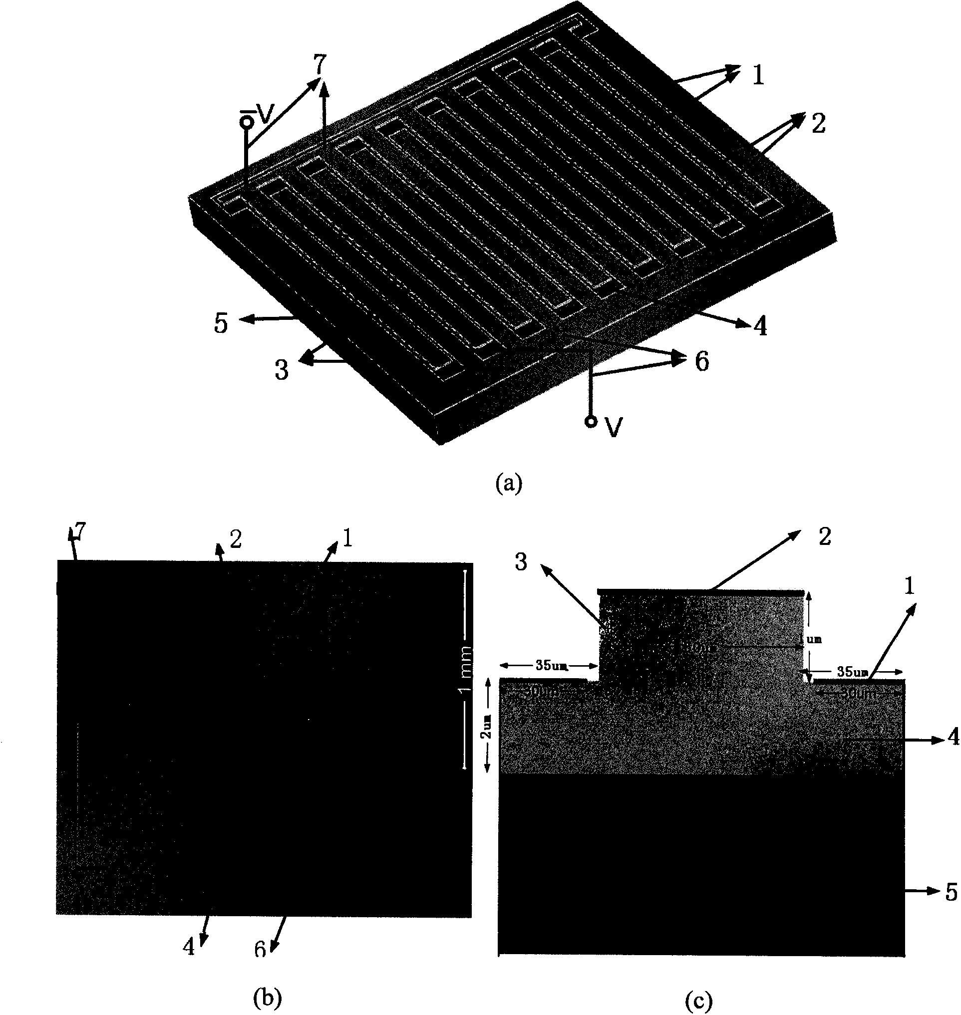
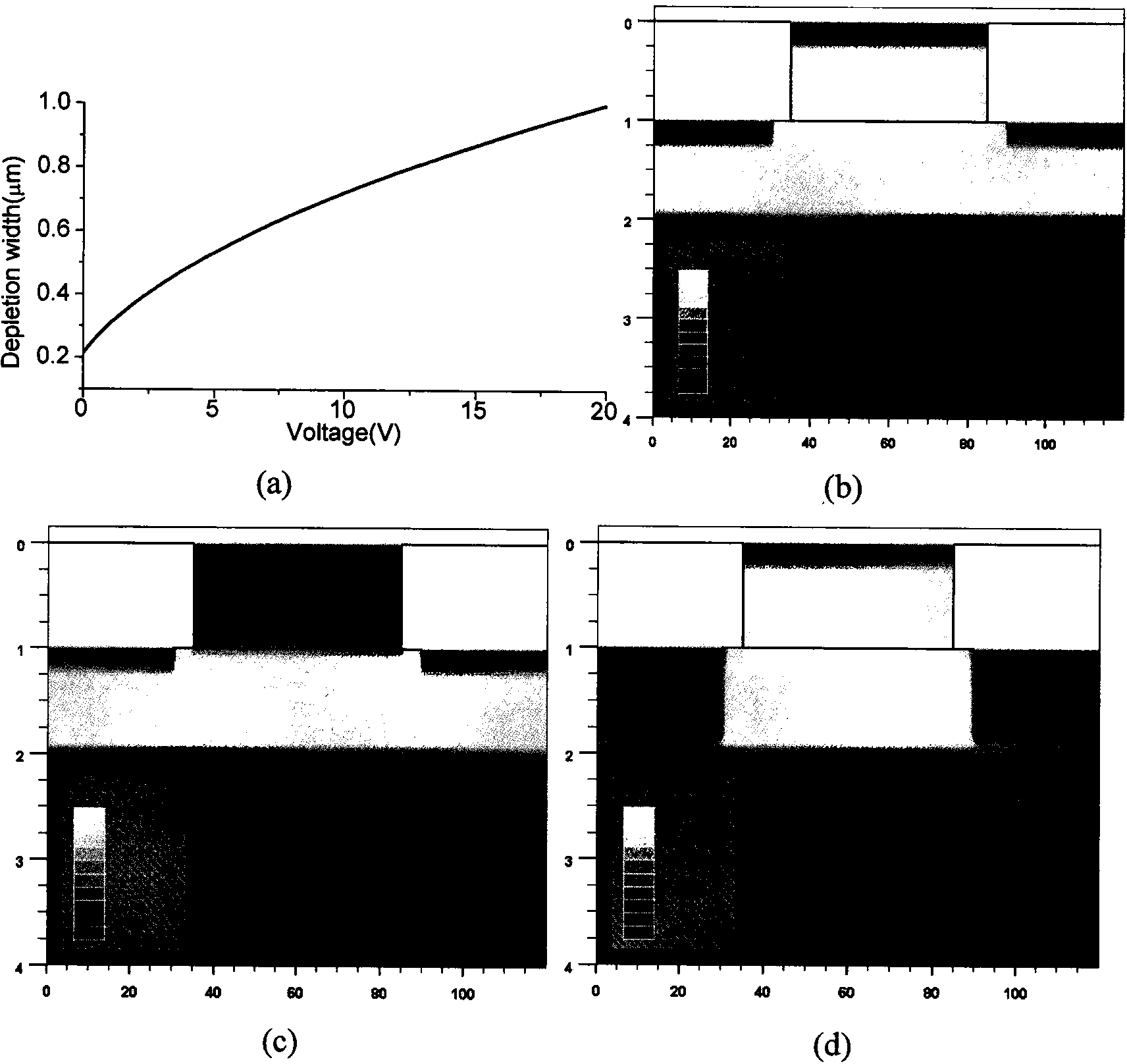
[0025] The working process of the present invention is illustrated by an example of a Schottky grid array terahertz modulator with a grid period of 120 μm and a grid width of 50 μm:

[0026] The structure of the device is as figure 1 As shown, epitaxially grown on a semi-insulating GaAs substrate with a thickness of 2 μm and a doping concentration of 3×10 16 cm -3 n-type doped gallium arsenide, etched gate steps with a period of 120 μm and a step width of 50 μm on the epitaxial layer to form a doped gallium arsenide epitaxial layer and gate steps with a height of 1 μm, the number of grids for 10 pcs. A 10nm-thick titanium and 100nm gold film is plated on the top of each gate-type step to form a stepped metal grid array; the same metal film is also plated on the doped gallium arsenide epitaxial layer to form a base metal grid array with a width of 60 μm, and the stepped metal grid The grid spacing is 5 μm. The base metal grid array is connected in series through the positiv...


PUM

PropertyMeasurementUnit
capacitanceaaaaaaaaaa

Abstract

The invention discloses a Schottky gate array type terahertz modulator and a regulation and control method thereof. A periodic gate type metal-semiconductor surface plasmon waveguide structure is adopted, the characteristics of Schottky contact formed by a metal-semiconductor interface and superposition of the Schottky contact and terahertz surface plasmon polariton position are utilized, a positive electrode and a negative electrode are led in and voltage is exerted, so that the terahertz modulation function of the Schottky gate array type terahertz modulator is achieved. The Schottky gate array type terahertz modulator combines a waveguide optical microstructure with a semiconductor electron device together, so that the Schottky gate array type terahertz modulator is well integrated with other electronic components and systems, and the optical functions of terahertz wave transmission and resonance oscillation are achieved. The Schottky gate array type terahertz modulator works from 2.2THz to 3.2THz, the working frequency can be tuned along with the working voltage, the maximum modulation depth is 16dB, and the highest modulation rate is 22MHz. The Schottky gate array type terahertz modulator is an on-chip electronically-controlled high-speed terahertz modulator which is in a small type and can be integrated, and the application requirements for terahertz broadband wireless communications are met.

Description

technical field [0001] The invention belongs to the technical field of terahertz applications, and in particular relates to a terahertz wave modulator and a control method thereof. Background technique [0002] Terahertz (1THz=10 12 THz) waves refer to electromagnetic waves with a frequency ranging from 0.1 to 10 THz (corresponding to a wavelength of 3 mm to 30 μm). This band is between microwaves and light waves, and is an intersecting field between electronics and photonics. Due to its special position in the electromagnetic spectrum, terahertz waves have many superior characteristics such as perspective, safety, and high signal-to-noise ratio, and have very important academic and application values ​​in the fields of spectroscopy, imaging, and communication. Terahertz communication has the advantages of large bandwidth, directivity, good confidentiality, and anti-electromagnetic interference. It can realize indoor short-distance or space confidential wireless communicati...

Claims


Application Information

Patent Timeline
Patent Type & Authority Applications(China)
IPC IPC(8): H04B10/54G02F1/015
Inventor 范飞常胜江
Owner NANKAI UNIV
Why Eureka
Try Eureka