Method for manufacturing high-resistance GaN thin film

A high-resistance, thin-film technology, applied in semiconductor/solid-state device manufacturing, electrical components, circuits, etc., can solve problems such as process complexity, reduction of material quality and electrical properties, and reaction chamber pollution

Inactive Publication Date: 2014-02-12
INST OF SEMICONDUCTORS - CHINESE ACAD OF SCI
View PDF6 Cites 19 Cited by
  • Summary
  • Abstract
  • Description
  • Claims
  • Application Information

AI Technical Summary

Problems solved by technology

However, these technologies have their own shortcomings, such as causing reaction chamber poll

Method used


Image

  • Method for manufacturing high-resistance GaN thin film
  • Method for manufacturing high-resistance GaN thin film

Examples


Embodiment Construction

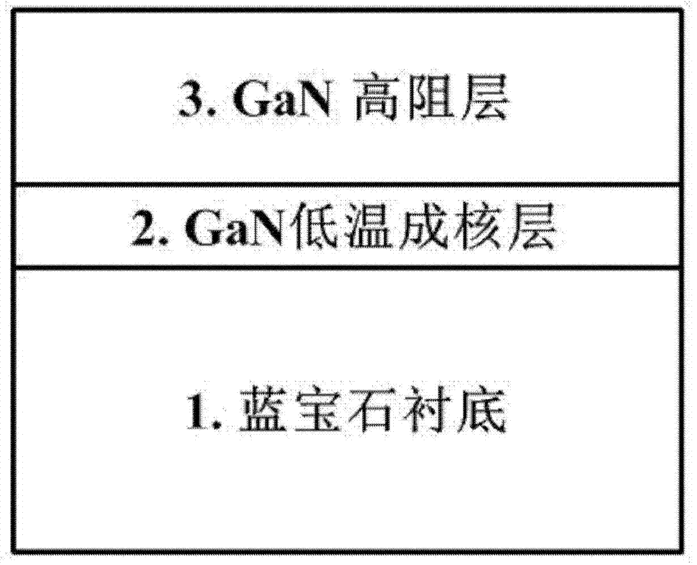
[0020] In order to make the object, technical solution and advantages of the present invention clearer, the present invention will be further described in detail below in conjunction with specific embodiments and with reference to the accompanying drawings. figure 1 A schematic diagram of the growth structure of a high-resistance GaN thin film proposed by the present invention is shown. Such as figure 1 As shown, the high-resistance GaN thin film includes from bottom to top:

[0021] A substrate 1, optionally, its material is sapphire;

[0022] A GaN low-temperature nucleation layer 2, which is fabricated on the substrate 1;

[0023] A GaN high resistance layer 3, the GaN high resistance layer 3 is fabricated on the GaN low temperature nucleation layer 2.

[0024] Among them, the above-mentioned high-resistance GaN film is grown by MOCVD equipment, trimethylgallium (TMGa) and ammonia (NH3) are used as gallium source and nitrogen source, hydrogen (H2) is used as carrier gas,...


PUM

PropertyMeasurementUnit
Growth temperatureaaaaaaaaaa

Abstract

The invention discloses a high-resistance GaN thin film and a method for manufacturing the high-resistance GaN thin film. The high-resistance GaN thin film comprises a substrate, a GaN low-temperature nucleating layer and a GaN high-resistance layer, wherein the GaN low-temperature nucleating layer is manufactured on the substrate, and the GaN high-resistance layer is manufactured on the GaN low-temperature nucleating layer. The high-resistance GaN thin film grows through MOCVD equipment, with trimethyl gallium and ammonia gas used as a gallium source and a nitrogen source, and with hydrogen used as carrier gas; the growth temperature of the GaN low-temperature nucleating layer is 550 DEG C, the pressure of a reaction chamber for the GaN low-temperature nucleating layer is 200 Torr, and the thickness of the GaN low-temperature nucleating layer ranges from 0.2 micrometer to 0.3 micrometer; the growth temperature of the GaN high-resistance layer is 1040 DEG C, the pressure of a reaction chamber for the GaN high-resistance layer is 50 Torr, and the thickness of the GaN high-resistance layer is 2 micrometers. According to the high-resistance GaN thin film, by controlling the pressure of the reaction chambers in the material growth process and controlling merging of carbon atoms in reaction precursors TMGa, carbon impurities are imported to acquire acceptor levels under the condition that a carbon source is not independently added, and background carrier concentration is compensated for.

Description

technical field [0001] The invention relates to the technical field of semiconductor materials, in particular to a preparation method of Gaozu GaH. Background technique [0002] In recent years, with the rise and rapid development of third-generation wireless communications and military phased array radars, high-power microwave devices such as high electron mobility transistors (HEMTs) have received extensive attention and research. GaN has excellent characteristics such as large band gap, high breakdown electric field, high electron saturation drift velocity, strong radiation resistance and good chemical stability; and it can form a heterojunction with AlGaN materials, and the pressure on the heterojunction interface Electric and spontaneous polarization can generate a high concentration of two-dimensional electron gas (2DEG), which is an excellent choice for fabricating HEMT devices. [0003] A basic HEMT device should have the following layers: substrate, nucleation laye...

Claims


Application Information

Patent Timeline
IPC IPC(8): H01L21/335H01L21/205
CPCH01L21/2056H01L29/66462
Inventor 何晓光赵德刚江德生刘宗顺陈平杨静乐伶聪李晓静杨辉
Owner INST OF SEMICONDUCTORS - CHINESE ACAD OF SCI
Why Eureka
Try Eureka