Structured light illumination microscopic imaging system based on silicon-based liquid crystal chip
A technology of structured light illumination and liquid crystal on silicon, which is applied in the field of imaging systems, can solve problems such as reducing system stability, and achieve the effects of avoiding impact, realizing portable design, and reducing system volume.
- Summary
- Abstract
- Description
- Claims
- Application Information
AI Technical Summary
Problems solved by technology
Method used
Image

Examples
Embodiment 1
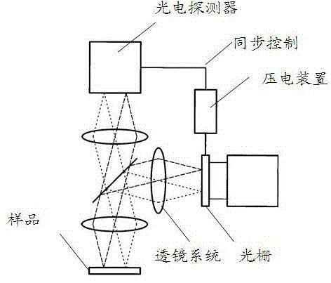
[0033] Such as figure 1 As shown in the figure, the working principle diagram of the structured illumination micro-imaging system using gratings in the current structure. The optical path is mainly composed of grating, illumination source, lens system, CCD and synchronous control system. The light emitted by the light source is collimated, and the structured light is generated by the grating to illuminate the surface of the object to be measured. The lens system images the fluorescence emitted by the object surface on the CCD plane. The piezoelectric device is used to synchronize the movement of the grating (corresponding to the phase shift) with the speed of the CCD recording image, that is, after an image is recorded, the grating moves a displacement to record the image corresponding to the new bit. The recorded images are reconstructed using a specific algorithm to obtain tomographic images and ultra-high-resolution two-dimensional images. This type of optical path has si...
Embodiment 2
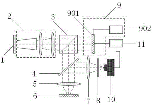
[0035] Such as figure 2 As shown, the structured light illumination super-resolution microscopy system using the liquid crystal-on-silicon chip LCoS development system 9 of the present invention, the light emitted from the high-brightness LED light source 1 is first collimated by the collimation module 2, and then enters the polarizing beam splitter In PBS3, the P-polarized light is transmitted and incident to the liquid crystal on silicon LCoS chip 901 , while the S-polarized light is reflected and cannot enter the optical path. The liquid crystal on silicon chip LCoS901 is controlled by the development system, and the target structure pattern is loaded to each pixel of the LCoS, so the incident S-polarized light is modulated, and when the pixel is in the "on" state of "1", the light passes through the pixel The polarization direction is rotated by 90 degrees, so as to become the P polarization state, which is reflected by the polarization beam splitter PBS3 and enters the o...
Embodiment 3
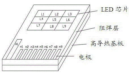
[0038] Such as image 3 As shown, a high-brightness LED module includes a high thermal conductivity substrate 1 and LED chips 2, the LED chips 2 are 2 LED chips with 9 groups of different central wavelengths, and the number of each group of LED chips 2 is at least one , the LED chip 2 is a common anode structure; the LED chip 2 is directly fixedly connected to the high thermal conductivity substrate 1 .
[0039] The central wavelength ranges of the nine LED chips 2 cover the ultraviolet band to the infrared band, and are individually controlled by independent control circuits. The control circuit includes a switch circuit that can control the circuit on and off of the corresponding group of LED chips, and also includes a current control circuit that controls the magnitude of the energizing current of the group of LED chips. Under the control of the driving circuit, single or multiple LED chips realize light emission.
PUM
 Abstract
Description
Claims
Application Information
PatSnap Eureka turns technology decisions into work you can execute. Powered by our Innovation Knowledge Graph, it runs expert workflows across engineering, life sciences, materials and intellectual property. Get your review-ready output in minutes.


